|
поискавой системы для электроныых деталей |
|
|
поискавой системы для электроныых деталей |
|
PIC16F631 датащи(PDF) 177 Page - Microchip Technology |
|
|
|||||||||||||||||||||||||||||
PIC16F631 датащи(HTML) 177 Page - Microchip Technology |
|
|
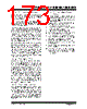
177 / 294 page  © 2007 Microchip Technology Inc. DS41262D-page 175 PIC16F631/677/685/687/689/690 13.0 SSP MODULE OVERVIEW The Synchronous Serial Port (SSP) module is a serial interface used to communicate with other peripheral or microcontroller devices. These peripheral devices may be serial EEPROMs, shift registers, display drivers, A/D converters, etc. The SSP module can operate in one of two modes: • Serial Peripheral Interface (SPI) • Inter-Integrated Circuit (I2C ™) Refer to Application Note AN578, “Use of the SSP Module in the Multi-Master Environment” (DS00578). 13.1 SPI Mode This section contains register definitions and operational characteristics of the SPI module. The SPI mode allows 8 bits of data to be synchronously transmitted and received simultaneously. To accomplish communication, typically three pins are used: • Serial Data Out (SDO) • Serial Data In (SDI) • Serial Clock (SCK) Additionally, a fourth pin may be used when in a Slave mode of operation: • Slave Select (SS) FIGURE 13-1: SSP BLOCK DIAGRAM (SPI MODE) Note 1: When the SPI is in Slave mode with SS pin control enabled (SSPM<3:0> bits of the SSPCON register = 0100), the SPI module will reset if the SS pin is set to VDD. 2: If the SPI is used in Slave mode with CKE = 1, then the SS pin control must be enabled. 3: When the SPI is in Slave mode with SS pin control enabled (SSPM<3:0> bits of the SSPCON register = 0100), the state of the SS pin can affect the state read back from the TRISC<4> bit. The peripheral OE signal from the SSP module into PORTC controls the state that is read back from the TRISC<4> bit (see Section 17.0 “Electrical Specifications” for information on PORTC). If read-write-modify instructions, such as BSF, are performed on the TRISC register while the SS pin is high, this will cause the TRISC<7> bit to be set, thus disabling the SDO output. Read Write Internal Data Bus SCK/ SSPSR Reg SSPBUF Reg SSPM<3:0> bit 0 Shift Clock SS Control Enable Edge Select Clock Select TMR2 Output TCY Prescaler 4, 16, 64 TRISB<6> 2 Edge Select 2 4 SCL Peripheral OE SDI/SDA SDO SS |
|
ссылки URL |
| Вашему бизинису помогли Аллдатащит? [ DONATE ] |
Что такое Аллдатащит | реклама | контакт | Конфиденциальность | Ссылка на техническое описание | обмен ссыками | поиск по производителю All Rights Reserved©Alldatasheet.com |
| Russian : Alldatasheetru.com | Korean : Alldatasheet.co.kr | Spanish : Alldatasheet.es | French : Alldatasheet.fr | Italian : Alldatasheetit.com Portuguese : Alldatasheetpt.com | Polish : Alldatasheet.pl | Vietnamese : Alldatasheet.vn Indian : Alldatasheet.in | Mexican : Alldatasheet.com.mx | British : Alldatasheet.co.uk | New Zealand : Alldatasheet.co.nz |
|
Family Site : ic2ic.com |
icmetro.com |
 Russian ▼
 English
 Chinese
 German
 Japanese
 Russian
 Korean
 Spanish
 French
 Italian
 Portuguese
 Polish
 Vietnamese
 Indian
 Mexican
 British
 New Zealand