|
поискавой системы для электроныых деталей |
|
|
поискавой системы для электроныых деталей |
|
PIC16F631 датащи(PDF) 206 Page - Microchip Technology |
|
|
|||||||||||||||||||||||||||||
PIC16F631 датащи(HTML) 206 Page - Microchip Technology |
|
|
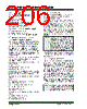
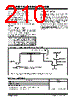
206 / 294 page  PIC16F631/677/685/687/689/690 DS41262D-page 204 © 2007 Microchip Technology Inc. 14.3 Interrupts The PIC16F631/677/685/687/689/690 have multiple sources of interrupt: • External Interrupt RA2/INT • TMR0 Overflow Interrupt • PORTA/PORTB Change Interrupts • 2 Comparator Interrupts • A/D Interrupt (except PIC16F631) • Timer1 Overflow Interrupt • Timer2 Match Interrupt (PIC16F685/PIC16F690 only) • EEPROM Data Write Interrupt • Fail-Safe Clock Monitor Interrupt • Enhanced CCP Interrupt (PIC16F685/PIC16F690 only) • EUSART Receive and Transmit interrupts (PIC16F687/PIC16F689/PIC16F690 only) The Interrupt Control register (INTCON) and Peripheral Interrupt Request Register 1 (PIR1) record individual interrupt requests in flag bits. The INTCON register also has individual and global interrupt enable bits. A Global Interrupt Enable bit, GIE (INTCON<7>), enables (if set) all unmasked interrupts, or disables (if cleared) all interrupts. Individual interrupts can be disabled through their corresponding enable bits in the INTCON, PIE1 and PIE2 registers, respectively. GIE is cleared on Reset. The Return from Interrupt instruction, RETFIE, exits the interrupt routine, as well as sets the GIE bit, which re-enables unmasked interrupts. The following interrupt flags are contained in the INTCON register: • INT Pin Interrupt • PORTA/PORTB Change Interrupts • TMR0 Overflow Interrupt The peripheral interrupt flags are contained in the PIR1 and PIR2 registers. The corresponding interrupt enable bits are contained in PIE1 and PIE2 registers. The following interrupt flags are contained in the PIR1 register: • A/D Interrupt • EUSART Receive and Transmit Interrupts • Timer1 Overflow Interrupt • Synchronous Serial Port (SSP) Interrupt • Enhanced CCP1 Interrupt • Timer1 Overflow Interrupt • Timer2 Match Interrupt The following interrupt flags are contained in the PIR2 register: • Fail-Safe Clock Monitor Interrupt • 2 Comparator Interrupts • EEPROM Data Write Interrupt When an interrupt is serviced: • The GIE is cleared to disable any further interrupt. • The return address is pushed onto the stack. • The PC is loaded with 0004h. For external interrupt events, such as the INT pin, PORTA/PORTB change interrupts, the interrupt latency will be three or four instruction cycles. The exact latency depends upon when the interrupt event occurs (see Figure 14-8). The latency is the same for one or two-cycle instructions. Once in the Interrupt Service Routine, the source(s) of the interrupt can be determined by polling the interrupt flag bits. The interrupt flag bit(s) must be cleared in software before re-enabling interrupts to avoid multiple interrupt requests. For additional information on Timer1, Timer2, comparators, A/D, data EEPROM, EUSART, SSP or Enhanced CCP modules, refer to the respective peripheral section. 14.3.1 RA2/INT INTERRUPT External interrupt on RA2/INT pin is edge-triggered; either rising if the INTEDG bit (OPTION_REG<6>) is set, or falling, if the INTEDG bit is clear. When a valid edge appears on the RA2/INT pin, the INTF bit (INTCON<1>) is set. This interrupt can be disabled by clearing the INTE control bit (INTCON<4>). The INTF bit must be cleared in software in the Interrupt Service Routine before re-enabling this interrupt. The RA2/INT interrupt can wake-up the processor from Sleep, if the INTE bit was set prior to going into Sleep. The status of the GIE bit decides whether or not the processor branches to the interrupt vector following wake-up (0004h). See Section 14.6 “Power-Down Mode (Sleep)” for details on Sleep and Figure 14-10 for timing of wake-up from Sleep through RA2/INT interrupt. Note 1: Individual interrupt flag bits are set, regardless of the status of their corresponding mask bit or the GIE bit. 2: When an instruction that clears the GIE bit is executed, any interrupts that were pending for execution in the next cycle are ignored. The interrupts, which were ignored, are still pending to be serviced when the GIE bit is set again. Note: The ANSEL and CM2CON0 registers must be initialized to configure an analog channel as a digital input. Pins configured as analog inputs will read ‘0’. |
|
ссылки URL |
| Вашему бизинису помогли Аллдатащит? [ DONATE ] |
Что такое Аллдатащит | реклама | контакт | Конфиденциальность | Ссылка на техническое описание | обмен ссыками | поиск по производителю All Rights Reserved©Alldatasheet.com |
| Russian : Alldatasheetru.com | Korean : Alldatasheet.co.kr | Spanish : Alldatasheet.es | French : Alldatasheet.fr | Italian : Alldatasheetit.com Portuguese : Alldatasheetpt.com | Polish : Alldatasheet.pl | Vietnamese : Alldatasheet.vn Indian : Alldatasheet.in | Mexican : Alldatasheet.com.mx | British : Alldatasheet.co.uk | New Zealand : Alldatasheet.co.nz |
|
Family Site : ic2ic.com |
icmetro.com |
 Russian ▼
 English
 Chinese
 German
 Japanese
 Russian
 Korean
 Spanish
 French
 Italian
 Portuguese
 Polish
 Vietnamese
 Indian
 Mexican
 British
 New Zealand