|
поискавой системы для электроныых деталей |
|
|
поискавой системы для электроныых деталей |
|
LT1794 датащи(PDF) 15 Page - Linear Technology |
|
|
|||||||||||||||||||||||||||||
LT1794 датащи(HTML) 15 Page - Linear Technology |
|
|
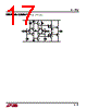
15 / 20 page  15 LT1794 Note that the overall gain is increased: V V RR R nR R R R R O I PP P FG P P P = + () + () + () []−+ () [] 22 1 12 1 11 1 / // / / A simpler method of using positive feedback to reduce the back-termination is shown in Figure 15. In this case, the drivers are driven differentially and provide complemen- tary outputs. Grounding the inputs, we see there is invert- ing gain of –RF/RP from –VO to VA VA = VO (RF/RP) and assuming RP >> RL, we require VA = VO (1 – 1/n) solving RF/RP = 1 – 1/n So to reduce the back-termination by a factor of 3 choose RF/RP = 2/3. Note that the overall gain is increased to: VO/VI = (1 + RF/RG + RF/RP)/[2(1 – RF/RP)] Using positive feedback is often referred to as active termination. Figure 17 shows a full-rate ADSL line driver incorporating positive feedback to reduce the power lost in the back termination resistors by 40% yet still maintains the proper impedance match to the100 Ω characteristic line imped- ance. This circuit also reduces the transformer turns ratio over the standard line driving approach resulting in lower peak current requirements. With lower current and less power loss in the back termination resistors, this driver dissipates only 1W of power, a 30% reduction. While the power savings of positive feedback are attractive there is one important system consideration to be ad- dressed, received signal sensitivity. The signal received from the line is sensed across the back termination resis- tors. With positive feedback, signals are present on both ends of the RBT resistors, reducing the sensed amplitude. Extra gain may be required in the receive channel to compensate, or a completely separate receive path may be implemented through a separate line coupling transformer. A demo board, DC306A, is available for the LT1794. This demo board is a complete line driver with an LT1361 receiver included. It allows the evaluation of both standard and active termination approaches. It also has circuitry built in to evaluate the effects of operating with reduced supply current. Considerations for Fault Protection The basic line driver design, shown on the front page of this data sheet, presents a direct DC path between the outputs of the two amplifiers. An imbalance in the DC biasing potentials at the noninverting inputs through either a fault condition or during turn-on of the system can create a DC voltage differential between the two amplifier outputs. This condition can force a considerable amount of current to flow as it is limited only by the small valued back-termination resistors and the DC resistance of the transformer primary. This high current can possibly cause the power supply voltage source to drop significantly impacting overall system performance. If left unchecked, the high DC current can heat the LT1794 to thermal shutdown. APPLICATIO S I FOR ATIO – + RBT RF RG RP RP RG RL RL –VI VA –VA VI –VO VO RBT 1794 F15 RF RL n = VO VI n = 1 – 2 FOR RBT = RF RP RF RP + RF RG 1 + 1 – RF RP 1 () Figure 15. Back Termination Using Differential Postive Feedback |
|
|
ссылки URL |
| Вашему бизинису помогли Аллдатащит? [ DONATE ] |
Что такое Аллдатащит | реклама | контакт | Конфиденциальность | Ссылка на техническое описание | обмен ссыками | поиск по производителю All Rights Reserved©Alldatasheet.com |
| Russian : Alldatasheetru.com | Korean : Alldatasheet.co.kr | Spanish : Alldatasheet.es | French : Alldatasheet.fr | Italian : Alldatasheetit.com Portuguese : Alldatasheetpt.com | Polish : Alldatasheet.pl | Vietnamese : Alldatasheet.vn Indian : Alldatasheet.in | Mexican : Alldatasheet.com.mx | British : Alldatasheet.co.uk | New Zealand : Alldatasheet.co.nz |
|
Family Site : ic2ic.com |
icmetro.com |
 Russian ▼
 English
 Chinese
 German
 Japanese
 Russian
 Korean
 Spanish
 French
 Italian
 Portuguese
 Polish
 Vietnamese
 Indian
 Mexican
 British
 New Zealand