|
поискавой системы для электроныых деталей |
|
|
поискавой системы для электроныых деталей |
|
LT1794 датащи(PDF) 13 Page - Linear Technology |
|
|
|||||||||||||||||||||||||||||
LT1794 датащи(HTML) 13 Page - Linear Technology |
|
|
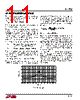
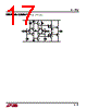
13 / 20 page  13 LT1794 Similar results can be obtained with the LT1794CSW in the wide SO-20 package. With this package heat is conducted primarily through the V– pins, Pins 4 to 7 and 14 to 17; these pins should be soldered directly to the PCB metal plane. Important Note: The metal planes used for heat sinking the LT1794 are electrically connected to the negative supply potential of the driver, typically – 12V. These planes must be isolated from any other power planes used in the board design. When PCB cards containing multiple ports are inserted into a rack in an enclosed cabinet, it is often necessary to provide airflow through the cabinet and over the cards. This is also very effective in reducing the junction-to- ambient thermal resistance of each line driver. To a limit, this thermal resistance can be reduced approximately 5 °C/W for every 100lfpm of laminar airflow. Layout and Passive Components With a gain bandwidth product of 200MHz the LT1794 requires attention to detail in order to extract maximum performance. Use a ground plane, short lead lengths and a combination of RF-quality supply bypass capacitors (i.e., 0.1 µF). As the primary applications have high drive cur- rent, use low ESR supply bypass capacitors (1 µF to 10µF). The parallel combination of the feedback resistor and gain setting resistor on the inverting input can combine with the input capacitance to form a pole that can cause frequency peaking. In general, use feedback resistors of 1k or less. Compensation The LT1794 is stable in a gain 10 or higher for any supply and resistive load. It is easily compensated for lower gains with a single resistor or a resistor plus a capacitor. Figure 9 shows that for inverting gains, a resistor from the inverting node to AC ground guarantees stability if the parallel combination of RC and RG is less than or equal to RF/9. For lowest distortion and DC output offset, a series capacitor, CC, can be used to reduce the noise gain at lower frequencies. The break frequency produced by RC and CC should be less than 5MHz to minimize peaking. Figure 10 shows compensation in the noninverting con- figuration. The RC, CC network acts similarly to the invert- ing case. The input impedance is not reduced because the network is bootstrapped. This network can also be placed between the inverting input and an AC ground. Another compensation scheme for noninverting circuits is shown in Figure 11. The circuit is unity gain at low frequency and a gain of 1 + RF/RG at high frequency. The DC output offset is reduced by a factor of ten. The techniques of Figures 10 and 11 can be combined as shown in Figure 12. The gain is unity at low frequencies, 1 + RF/RG at mid-band and for stability, a gain of 10 or greater at high frequencies. Figure 9. Compensation for Inverting Gains APPLICATIO S I FOR ATIO RG RC VO VI CC (OPTIONAL) 1794 F09 RF = –RF RG VO VI < 5MHz 1 2 πRCCC (RC || RG) ≤ RF/9 RC VO VI CC (OPTIONAL) 1794 F10 RF RG = 1 + RF RG VO VI < 5MHz 1 2 πRCCC (RC || RG) ≤ RF/9 Figure 10. Compensation for Noninverting Gains 1794 F11 RF RG Vi VO CC < 5MHz 1 2 πRGCC RG ≤ RF/9 = 1 (LOW FREQUENCIES) (HIGH FREQUENCIES) VO VI = 1 + RF RG Figure 11. Alternate Noninverting Compensation |
|
|
ссылки URL |
| Вашему бизинису помогли Аллдатащит? [ DONATE ] |
Что такое Аллдатащит | реклама | контакт | Конфиденциальность | Ссылка на техническое описание | обмен ссыками | поиск по производителю All Rights Reserved©Alldatasheet.com |
| Russian : Alldatasheetru.com | Korean : Alldatasheet.co.kr | Spanish : Alldatasheet.es | French : Alldatasheet.fr | Italian : Alldatasheetit.com Portuguese : Alldatasheetpt.com | Polish : Alldatasheet.pl | Vietnamese : Alldatasheet.vn Indian : Alldatasheet.in | Mexican : Alldatasheet.com.mx | British : Alldatasheet.co.uk | New Zealand : Alldatasheet.co.nz |
|
Family Site : ic2ic.com |
icmetro.com |
 Russian ▼
 English
 Chinese
 German
 Japanese
 Russian
 Korean
 Spanish
 French
 Italian
 Portuguese
 Polish
 Vietnamese
 Indian
 Mexican
 British
 New Zealand