|
поискавой системы для электроныых деталей |
|
|
поискавой системы для электроныых деталей |
|
LT1794 датащи(PDF) 9 Page - Linear Technology |
|
|
|||||||||||||||||||||||||||||
LT1794 датащи(HTML) 9 Page - Linear Technology |
|
|
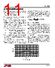
9 / 20 page  9 LT1794 Two Control Inputs RESISTOR VALUES (k Ω) RSHDN TO VCC (12V) RSHDN TO VLOGIC VLOGIC RSHDN RC1 RCO 3V 40.2 11.5 19.1 3.3V 43.2 13.0 22.1 5V 60.4 21.5 36.5 3V 4.99 8.66 14.3 3.3V 6.81 10.7 17.8 5V 19.6 20.5 34.0 VC0 H L H L VC1 H H L L 10 7 5 2 10 7 5 2 10 7 5 2 10 7 5 2 10 7 5 2 10 7 5 2 SUPPLY CURRENT PER AMPLIFIER (mA) One Control Input RESISTOR VALUES (k Ω) RSHDN TO VCC (12V) RSHDN TO VLOGIC VLOGIC RSHDN RC 3V 40.2 7.32 3.3V 43.2 8.25 5V 60.4 13.7 3V 4.99 5.49 3.3V 6.81 6.65 5V 19.6 12.7 VC H L 10 2 10 2 10 2 10 2 10 2 10 2 SUPPLY CURRENT PER AMPLIFIER (mA) RSHDN RC1 VC1 VLOGIC 12V OR VLOGIC 0V VC0 RC0 SHDN SHDNREF 2k RSHDN RC VC VLOGIC 12V OR VLOGIC 0V SHDN SHDNREF 1794 F04 2k APPLICATIO S I FOR ATIO Logic Controlled Operating Current The DSP controller in a typical xDSL application can have I/O pins assigned to provide logic control of the LT1794 line driver operating current. As shown in Figure 4 one or two logic control inputs can control two or four different operating modes. The logic inputs add or subtract current to the SHDN input to set the operating current. The one logic input example selects the supply current to be either full power, 10mA per amplifier or just 2mA per amplifier, which significantly reduces the driver power consumption while maintaining less than 2 Ω output impedance to frequencies less than 1MHz. This low power mode retains termination impedance at the amplifier outputs and the line driving back termination resistors. With this termina- tion, while a DSL port is not transmitting data, it can still sense a received signal from the line across the back- termination resistors and respond accordingly. The two logic input control provides two intermediate (approximately 7mA per amplifier and 5mA per amplifier) operating levels between full power and termination modes. These modes can be useful for overall system power management when full power transmissions are not necessary. Shutdown and Recovery The ultimate power saving action on a completely idle port is to fully shut down the line driver by pulling the SHDN pin to within 0.4V of the SHDNREF potential. As shown in Figure 5 complete shutdown occurs in less than 10 µs and, more importantly, complete recovery from the shut down state to full operation occurs in less than 2 µs. The biasing circuitry in the LT1794 reacts very quickly to bring the amplifiers back to normal operation. Figure 4. Providing Logic Input Control of Operating Current VSHDN SHDNREF = 0V AMPLIFIER OUTPUT 1794 F05 Figure 5. Shutdown and Recovery Timing |
|
|
ссылки URL |
| Вашему бизинису помогли Аллдатащит? [ DONATE ] |
Что такое Аллдатащит | реклама | контакт | Конфиденциальность | Ссылка на техническое описание | обмен ссыками | поиск по производителю All Rights Reserved©Alldatasheet.com |
| Russian : Alldatasheetru.com | Korean : Alldatasheet.co.kr | Spanish : Alldatasheet.es | French : Alldatasheet.fr | Italian : Alldatasheetit.com Portuguese : Alldatasheetpt.com | Polish : Alldatasheet.pl | Vietnamese : Alldatasheet.vn Indian : Alldatasheet.in | Mexican : Alldatasheet.com.mx | British : Alldatasheet.co.uk | New Zealand : Alldatasheet.co.nz |
|
Family Site : ic2ic.com |
icmetro.com |
 Russian ▼
 English
 Chinese
 German
 Japanese
 Russian
 Korean
 Spanish
 French
 Italian
 Portuguese
 Polish
 Vietnamese
 Indian
 Mexican
 British
 New Zealand