 |
поискавой системы для электроныых деталей |
|
|
поискавой системы для электроныых деталей |
|
The question interval is too short.
Please try again in a few seconds.

Hello, Please ask a question about 80VA Datasheet
# Example questions:
➢ What is the maximum junction temperature (tj) for the device?
➢ What does the documentation state regarding the implications of exceeding the 'absolute maximum ratings'?
➢ What type of documentation should be consulted for thermal management guidelines?
| Part No. | 80VA |
| Manufacturer | LATTICE |
| Size | 346 Kbytes |
| Pages | 27 pages |
| Description | In-System Programmable 3.3V Generic Digital CrosspointTM |


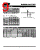
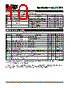


This is a challenging set of images to process as the text is very dense, repetitive, and spans multiple pages with overlapping information. Here's a breakdown of what I can extract and summarize, along with the limitations:
Overall Summary:
These documents appear to be data sheets or technical documentation for Lattice Semiconductor devices, specifically concerning I/O Management and routing within a programmable logic device (likely a FPGA). The documentation focuses on a feature called "Routing and I/O Architecture", specifically dealing with how signals are directed and managed within the device's input/output (I/O) circuitry. The information is extremely detailed and geared towards engineers who design and implement digital systems using these devices.
Key Points & Data (as best I can decipher):
1. Routing Architecture:
- The document describes how signals are routed to and from I/O pins.
- This involves an architecture with "routing resources" – implying flexible connection paths.
- There's an emphasis on configurable routing, which is characteristic of FPGAs.
2. I/O Management:
- The architecture allows for multiple functions to be assigned to single I/O pins, increasing density.
- Signals can be routed as inputs, outputs, or bidirectional.
- There's mention of signal buffering and level shifting for compatibility.
3. I/O Standards: The device supports a variety of I/O standards including:
- LVTTL
- HSTL
- HSTL_II
- PCI
- Many more. These standards dictate voltage levels, timing, and other electrical characteristics.
4. Absolute Maximum Ratings (Electrical Specs): This appears from one of the pages, showing voltage ranges and temperature limits. These are critical for preventing damage to the device.
5. Routing Table & Mappings: There are pages containing tables that detail the routing options available for specific I/O pins. These are essential for configuration.
6. Page Numbers & Repetitions: The documentation repeats similar information across multiple pages, which can make it difficult to distinguish between primary content and reiteration.
Limitations and Challenges:
️· Image Quality: Some images are blurry or have overlapping text, making accurate transcription and interpretation difficult.
️· Dense Text: The text is very dense and technical.
️· Repetitive Information: There's a lot of repetition across pages.
️· Page Breaks: Key relationships between pages may be lost due to cuts.
️· Technical Jargon: Requires a deep understanding of FPGA architecture and digital circuit design to fully understand.
To improve this summary, you would need:
️· Higher-resolution images.
️· The full, complete document as a PDF.
️· Knowledge of the specific Lattice Semiconductor device being documented.
Please provide more questions if you would like me to focus on a specific section of the information or elaborate on any details.
This is a challenging set of images to process as the text is very dense, repetitive, and spans multiple pages with overlapping information. Here's a breakdown of what I can extract and summarize, along with the limitations:
Overall Summary:
These documents appear to be data sheets or technical documentation for Lattice Semiconductor devices, specifically concerning I/O Management and routing within a programmable logic device (likely a FPGA). The documentation focuses on a feature called "Routing and I/O Architecture", specifically dealing with how signals are directed and managed within the device's input/output (I/O) circuitry. The information is extremely detailed and geared towards engineers who design and implement digital systems using these devices.
Key Points & Data (as best I can decipher):
1. Routing Architecture:
- The document describes how signals are routed to and from I/O pins.
- This involves an architecture with "routing resources" – implying flexible connection paths.
- There's an emphasis on configurable routing, which is characteristic of FPGAs.
2. I/O Management:
- The architecture allows for multiple functions to be assigned to single I/O pins, increasing density.
- Signals can be routed as inputs, outputs, or bidirectional.
- There's mention of signal buffering and level shifting for compatibility.
3. I/O Standards: The device supports a variety of I/O standards including:
- LVTTL
- HSTL
- HSTL_II
- PCI
- Many more. These standards dictate voltage levels, timing, and other electrical characteristics.
4. Absolute Maximum Ratings (Electrical Specs): This appears from one of the pages, showing voltage ranges and temperature limits. These are critical for preventing damage to the device.
5. Routing Table & Mappings: There are pages containing tables that detail the routing options available for specific I/O pins. These are essential for configuration.
6. Page Numbers & Repetitions: The documentation repeats similar information across multiple pages, which can make it difficult to distinguish between primary content and reiteration.
Limitations and Challenges:
️· Image Quality: Some images are blurry or have overlapping text, making accurate transcription and interpretation difficult.
️· Dense Text: The text is very dense and technical.
️· Repetitive Information: There's a lot of repetition across pages.
️· Page Breaks: Key relationships between pages may be lost due to cuts.
️· Technical Jargon: Requires a deep understanding of FPGA architecture and digital circuit design to fully understand.
To improve this summary, you would need:
️· Higher-resolution images.
️· The full, complete document as a PDF.
️· Knowledge of the specific Lattice Semiconductor device being documented.
Please provide more questions if you would like me to focus on a specific section of the information or elaborate on any details.
| Part No. | 80VA |
| Manufacturer | LATTICE |
| Size | 346 Kbytes |
| Pages | 27 pages |
| Description | In-System Programmable 3.3V Generic Digital CrosspointTM |
| Вашему бизинису помогли Аллдатащит? [ DONATE ] |
Что такое Аллдатащит | реклама | контакт | Конфиденциальность | Ссылка на техническое описание | обмен ссыками | поиск по производителю All Rights Reserved©Alldatasheet.com |
| Russian : Alldatasheetru.com | Korean : Alldatasheet.co.kr | Spanish : Alldatasheet.es | French : Alldatasheet.fr | Italian : Alldatasheetit.com Portuguese : Alldatasheetpt.com | Polish : Alldatasheet.pl | Vietnamese : Alldatasheet.vn Indian : Alldatasheet.in | Mexican : Alldatasheet.com.mx | British : Alldatasheet.co.uk | New Zealand : Alldatasheet.co.nz |
|
Family Site : ic2ic.com |
icmetro.com |
 Russian ▼
  English
 Chinese
 German
 Japanese
 Korean
 Spanish
 French
 Italian
 Portuguese
 Polish
 Vietnamese
 Indian
 Mexican
 British
 New Zealand