|
поискавой системы для электроныых деталей |
|
|
поискавой системы для электроныых деталей |
|
PIC16LC71 датащи(PDF) 145 Page - Microchip Technology |
|
|
|||||||||||||||||||||||||||||
PIC16LC71 датащи(HTML) 145 Page - Microchip Technology |
|
|
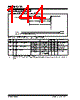
145 / 176 page  © 1997 Microchip Technology Inc. DS30272A-page 145 PIC16C71X Applicable Devices 710 71 711 715 TABLE 15-6: A/D CONVERTER CHARACTERISTICS Param No. Sym Characteristic Min Typ† Max Units Conditions A01 NR Resolution — — 8 bits bits VREF = VDD = 5.12V, VSS ≤ VAIN ≤ VREF A02 EABS Absolute error PIC16C71 — — < ±1 LSb VREF = VDD = 5.12V, VSS ≤ VAIN ≤ VREF PIC16LC71 — — < ±2 LSb VREF = VDD = 3.0V (Note 3) A03 EIL Integral linearity error PIC16C71 — — < ±1 LSb VREF = VDD = 5.12V, VSS ≤ VAIN ≤ VREF PIC16LC71 — — < ±2 LSb VREF = VDD = 3.0V (Note 3) A04 EDL Differential linearity error PIC16C71 — — < ±1 LSb VREF = VDD = 5.12V, VSS ≤ VAIN ≤ VREF PIC16LC71 — — < ±2 LSb VREF = VDD = 3.0V (Note 3) A05 EFS Full scale error PIC16C71 — — < ±1 LSb VREF = VDD = 5.12V, VSS ≤ VAIN ≤ VREF PIC16LC71 — — < ±2 LSb VREF = VDD = 3.0V (Note 3) A06 EOFF Offset error PIC16C71 — — < ±1 LSb VREF = VDD = 5.12V, VSS ≤ VAIN ≤ VREF PIC16LC71 — — < ±2 LSb VREF = VDD = 3.0V (Note 3) A10 — Monotonicity — guaranteed — — VSS ≤ VAIN ≤ VREF A20 VREF Reference voltage 3.0V — VDD + 0.3 V A25 VAIN Analog input voltage VSS - 0.3 — VREF V A30 ZAIN Recommended impedance of analog voltage source — — 10.0 k Ω A40 IAD A/D conversion current (VDD) — 180 — µA Average current consump- tion when A/D is on. (Note 1) A50 IREF VREF input current (Note 2) PIC16C71 10 — — — 1000 40 µA µA During VAIN acquisition. Based on differential of VHOLD to VAIN. To charge CHOLD see Section 7.1. During A/D Conversion cycle PIC16LC71 — — — — 1 10 mA µA During VAIN acquisition. Based on differential of VHOLD to VAIN. To charge CHOLD see Section 7.1. During A/D Conversion cycle * These parameters are characterized but not tested. † Data in “Typ” column is at 5V, 25 °C unless otherwise stated. These parameters are for design guidance only and are not tested. Note 1: When A/D is off, it will not consume any current other than minor leakage current. The power-down current spec includes any such leakage from the A/D module. 2: VREF current is from RA3 pin or VDD pin, whichever is selected as reference input. 3: These specifications apply if VREF = 3.0V and if VDD ≥ 3.0V. VAIN must be between VSS and VREF. |
|
ссылки URL |
| Вашему бизинису помогли Аллдатащит? [ DONATE ] |
Что такое Аллдатащит | реклама | контакт | Конфиденциальность | Ссылка на техническое описание | обмен ссыками | поиск по производителю All Rights Reserved©Alldatasheet.com |
| Russian : Alldatasheetru.com | Korean : Alldatasheet.co.kr | Spanish : Alldatasheet.es | French : Alldatasheet.fr | Italian : Alldatasheetit.com Portuguese : Alldatasheetpt.com | Polish : Alldatasheet.pl | Vietnamese : Alldatasheet.vn Indian : Alldatasheet.in | Mexican : Alldatasheet.com.mx | British : Alldatasheet.co.uk | New Zealand : Alldatasheet.co.nz |
|
Family Site : ic2ic.com |
icmetro.com |
 Russian ▼
 English
 Chinese
 German
 Japanese
 Russian
 Korean
 Spanish
 French
 Italian
 Portuguese
 Polish
 Vietnamese
 Indian
 Mexican
 British
 New Zealand