|
поискавой системы для электроныых деталей |
|
|
поискавой системы для электроныых деталей |
|
PIC16LC71 датащи(PDF) 42 Page - Microchip Technology |
|
|
|||||||||||||||||||||||||||||
PIC16LC71 датащи(HTML) 42 Page - Microchip Technology |
|
|
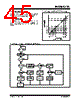
42 / 176 page  PIC16C71X DS30272A-page 42 © 1997 Microchip Technology Inc. 7.4 A/D Conversions Example 7-2 shows how to perform an A/D conversion. The RA pins are configured as analog inputs. The ana- log reference (VREF) is the device VDD. The A/D inter- rupt is enabled, and the A/D conversion clock is FRC. The conversion is performed on the RA0 pin (channel 0). Clearing the GO/DONE bit during a conversion will abort the current conversion. The ADRES register will NOT be updated with the partially completed A/D con- version sample. That is, the ADRES register will con- tinue to contain the value of the last completed conversion (or the last value written to the ADRES reg- ister). After the A/D conversion is aborted, a 2TAD wait is required before the next acquisition is started. After this 2TAD wait, an acquisition is automatically started on the selected channel. Note: The GO/DONE bit should NOT be set in the same instruction that turns on the A/D. EXAMPLE 7-2: A/D CONVERSION BSF STATUS, RP0 ; Select Bank 1 CLRF ADCON1 ; Configure A/D inputs BCF STATUS, RP0 ; Select Bank 0 MOVLW 0xC1 ; RC Clock, A/D is on, Channel 0 is selected MOVWF ADCON0 ; BSF INTCON, ADIE ; Enable A/D Interrupt BSF INTCON, GIE ; Enable all interrupts ; ; Ensure that the required sampling time for the selected input channel has elapsed. ; Then the conversion may be started. ; BSF ADCON0, GO ; Start A/D Conversion : ; The ADIF bit will be set and the GO/DONE bit : ; is cleared upon completion of the A/D Conversion. |
|
ссылки URL |
| Вашему бизинису помогли Аллдатащит? [ DONATE ] |
Что такое Аллдатащит | реклама | контакт | Конфиденциальность | Ссылка на техническое описание | обмен ссыками | поиск по производителю All Rights Reserved©Alldatasheet.com |
| Russian : Alldatasheetru.com | Korean : Alldatasheet.co.kr | Spanish : Alldatasheet.es | French : Alldatasheet.fr | Italian : Alldatasheetit.com Portuguese : Alldatasheetpt.com | Polish : Alldatasheet.pl | Vietnamese : Alldatasheet.vn Indian : Alldatasheet.in | Mexican : Alldatasheet.com.mx | British : Alldatasheet.co.uk | New Zealand : Alldatasheet.co.nz |
|
Family Site : ic2ic.com |
icmetro.com |
 Russian ▼
 English
 Chinese
 German
 Japanese
 Russian
 Korean
 Spanish
 French
 Italian
 Portuguese
 Polish
 Vietnamese
 Indian
 Mexican
 British
 New Zealand