|
поискавой системы для электроныых деталей |
|
|
поискавой системы для электроныых деталей |
|
SSM2160P датащи(PDF) 5 Page - Analog Devices |
|
|
|||||||||||||||||||||||||||||
SSM2160P датащи(HTML) 5 Page - Analog Devices |
|
|
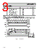
5 / 16 page  SSM2160/SSM2161 –5– REV. 0 PIN DESCRIPTIONS SSM2160 SSM2161 Pin No. Pin No. Name Function 1 1 V+ V+ is the positive power supply pin. Refer to the Power Supply Connections section for more information. 2 2 AGND AGND is the internal ground reference for the audio circuitry. When operating the SSM2160 from dual supplies, AGND should be connected to ground. When operating from a single supply, AGND should be connected to VREF, the internally generated voltage reference. AGND may also be connected to an external reference. Refer to the Power Supply Connections section for more details. 33 VREF VREF is the internally generated ground reference for the audio circuitry obtained from a buffered divider between V+ and V–. In a dual-supply application with the AGND pin connected to ground, VREF should be left floating. In a single supply application, VREF should be connected to AGND. Refer to the Power Supply Connections section for more details. 4 4 CH1 OUT Audio Output from Channel 1. 5 5 CH1 IN Audio Input to Channel 1. 6 6 CH3 OUT Audio Output from Channel 3. 7 7 CH3 IN Audio Input to Channel 3. 8 – CH5 OUT Audio Output from Channel 5. 9 – CH5 IN Audio Input to Channel 5. 10 8 WRITE A logic LOW voltage enables the SSM2160 to receive information at the DATA input (Pin 15). A logic HIGH applied to WRITE retains data at their previous settings. See Timing Diagrams. Serves as CHIP SELECT. 11 9 LD Loads the information retained by WRITE into the SSM2160 at logic LOW. See Timing Diagrams. 12 10 V– V– is the negative power supply pin. Connect to ground if using in a single supply application. Refer to the Power Supply Connections section for more details. 13 11 DGND DGND is the digital ground reference for the SSM2160. This pin should always be connected to ground. All digital inputs, including WRITE, LD, CLK, and DATA are TTL input compatible; drive currents are returned to DGND. 14 12 CLK CLK is the clock input. It is positive edge triggered. See Timing Diagrams. 15 13 DATA Channel and Master control information flows MSB first into the DATA pin. Refer to Address/ Data Decoding Truth Table, Figure 19, for information on how to control the VCAs. 16 – CH6 IN Audio Input to Channel 6. 17 – CH6 OUT Audio Output from Channel 6. 18 14 CH4 IN Audio Input to Channel 4. 19 15 CH4 OUT Audio Output from Channel 4. 20 16 CH2 IN Audio Input to Channel 2. 21 17 CH2 OUT Audio Output from Channel 2. 22 18 MSTR SET MSTR SET is connected to the inverting input of an I-V converting op amp used to generate a Master Control voltage from the Master Control DAC current output. A resistor connected from MSTR OUT to MSTR SET reduces the step size of the Master control. See the Adjusting Step Sizes section for more details. A 10 µF capacitor should be connected from MSTR OUT to MSTR SET to eliminate the zipper noise in the Master control. 23 19 MSTR OUT MSTR OUT is connected to the output of the I-V converting op amp. See MSTR SET description. 24 20 CH SET The step size of the Channel Control can be increased by connecting a resistor from CH SET to V+. No connection to CH SET is required if the default value of 1 dB per step is desired. Mini- mum of 10 Ω external resistor. See the Adjusting Step Sizes section for more details. |
|
|
ссылки URL |
| Вашему бизинису помогли Аллдатащит? [ DONATE ] |
Что такое Аллдатащит | реклама | контакт | Конфиденциальность | Ссылка на техническое описание | обмен ссыками | поиск по производителю All Rights Reserved©Alldatasheet.com |
| Russian : Alldatasheetru.com | Korean : Alldatasheet.co.kr | Spanish : Alldatasheet.es | French : Alldatasheet.fr | Italian : Alldatasheetit.com Portuguese : Alldatasheetpt.com | Polish : Alldatasheet.pl | Vietnamese : Alldatasheet.vn Indian : Alldatasheet.in | Mexican : Alldatasheet.com.mx | British : Alldatasheet.co.uk | New Zealand : Alldatasheet.co.nz |
|
Family Site : ic2ic.com |
icmetro.com |
 Russian ▼
 English
 Chinese
 German
 Japanese
 Russian
 Korean
 Spanish
 French
 Italian
 Portuguese
 Polish
 Vietnamese
 Indian
 Mexican
 British
 New Zealand