|
поискавой системы для электроныых деталей |
|
|
поискавой системы для электроныых деталей |
|
LTC4155 датащи(PDF) 45 Page - Linear Technology |
|
|
|||||||||||||||||||||||||||||
LTC4155 датащи(HTML) 45 Page - Linear Technology |
|
|
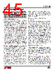
45 / 52 page  LTC4155 45 4155fc Table 38. Recommended P-Channel Battery Charger MOSFETs MANUFACTURER PART NUMBER RDS(ON) (mΩ) VT (V) BVDSS (V) Fairchild FDMC510P 7.6 –0.5 –20 Vishay Si7123DN 11.2 –1 –20 Vishay Si5481DU 24 –1 –20 VBUS and VOUT Bypass Capacitors The style and value of the capacitors used with the LTC4155 determine several important parameters such as regulator control loop stability and input voltage ripple. Because the LTC4155 uses a step-down switching power supply from VBUS to VOUT, its input current waveform contains high frequency components. It is strongly recommended that a low equivalent series resistance (ESR) multilayer ceramic capacitor be used to bypass VBUS. Tantalum and aluminum capacitors are not recommended because of their high ESR. The value of the capacitor on VBUS directly controls the amount of input ripple for a given load current. Increasing the size of this capacitor will reduce the input ripple. The USB specification allows a maximum of 10μF to be connected directly across the USB power bus. If the overvoltage protection circuit is used to protect VBUS, then its soft-starting nature can be exploited and a larger VBUS capacitor can be used if desired. If one or both of the input channels are never used for USB, additional capacitance placed upstream of the overvoltage protection NMOS de- vices can absorb significant high frequency current ripple. To prevent large VOUT voltage steps during transient load conditions, it is also recommended that a ceramic capacitor be used to bypass VOUT. The output capacitor is used in the compensation of the switching regulator. At least 22μF with low ESR are required on VOUT. Additional capacitance will improve load transient performance and stability. Multilayer ceramic chip capacitors typically have excep- tional ESR performance. MLCCs combined with a tight board layout and an unbroken ground plane will yield very good performance and low EMI emissions. The actual in-circuit capacitance of a ceramic capacitor should be measured with a small AC signal and DC bias, as is expected in-circuit. Many vendors specify the capaci- tance versus voltage with a 1VRMS AC test signal and, as a result, overstate the capacitance that the capacitor will present in the application. Using similar operating condi- tions as the application, the user must measure, or request from the vendor, the actual capacitance to determine if the selected capacitor meets the minimum capacitance that the application requires. Programming the Input and Battery Charge Current Limits The LTC4155 features independent resistor programma- bility of the input current limit and battery charge current limit to facilitate optimal charging from a wide variety of input power sources. The battery charge current should be programmed based on the size of the battery and its associated safe charging rate. Typically this rate is close to “1C”, or equal to the current which would discharge the battery in one hour. For example, a 2000mAH battery would be charged with no more than 2A. With the full- scale (default) charge current programmed with a resistor between PROG and GND, all other I2C selectable charge current settings are lower and may be appropriate for cus- tom charge algorithms at extreme temperature or battery voltage. If the battery charge current limit requires more power than is available from the selected input current limit, the input current limit will be enforced and the battery will charge with less than the programmed current. Thus, the battery charger should be programmed optimally for the battery without concern for the input source. Resistive Inputs and Test Equipment Care must be exercised in the laboratory while evaluat- ing the LTC4155 with inline ammeters. The combined resistance of the internal current sense resistor and fuse of many meters can be 0.5Ω or more. At currents of 3A to 4A, it is possible to drop several volts across the meter, possibly resulting in unusual voltage readings or artificially high switch duty cycles. A resistive connection to the source of input power can be particularly troublesome. With the undervoltage cur- rent limit feature enabled, the switching regulator output power will be automatically reduced to prevent VBUS from falling below 4.3V. This feature greatly improves tolerance of resistive input power sources (from either undersized wiring and connectors or test equipment) and facilitates APPLICATIONS INFORMATION |
|
ссылки URL |
| Вашему бизинису помогли Аллдатащит? [ DONATE ] |
Что такое Аллдатащит | реклама | контакт | Конфиденциальность | Ссылка на техническое описание | обмен ссыками | поиск по производителю All Rights Reserved©Alldatasheet.com |
| Russian : Alldatasheetru.com | Korean : Alldatasheet.co.kr | Spanish : Alldatasheet.es | French : Alldatasheet.fr | Italian : Alldatasheetit.com Portuguese : Alldatasheetpt.com | Polish : Alldatasheet.pl | Vietnamese : Alldatasheet.vn Indian : Alldatasheet.in | Mexican : Alldatasheet.com.mx | British : Alldatasheet.co.uk | New Zealand : Alldatasheet.co.nz |
|
Family Site : ic2ic.com |
icmetro.com |
 Russian ▼
 English
 Chinese
 German
 Japanese
 Russian
 Korean
 Spanish
 French
 Italian
 Portuguese
 Polish
 Vietnamese
 Indian
 Mexican
 British
 New Zealand