|
поискавой системы для электроныых деталей |
|
|
поискавой системы для электроныых деталей |
|
PIC16F631 датащи(PDF) 171 Page - Microchip Technology |
|
|
|||||||||||||||||||||||||||||
PIC16F631 датащи(HTML) 171 Page - Microchip Technology |
|
|
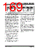
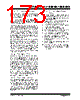
171 / 294 page  © 2007 Microchip Technology Inc. DS41262D-page 169 PIC16F631/677/685/687/689/690 12.4 EUSART Synchronous Mode Synchronous serial communications are typically used in systems with a single master and one or more slaves. The master device contains the necessary cir- cuitry for baud rate generation and supplies the clock for all devices in the system. Slave devices can take advantage of the master clock by eliminating the internal clock generation circuitry. There are two signal lines in Synchronous mode: a bidi- rectional data line and a clock line. Slaves use the external clock supplied by the master to shift the serial data into and out of their respective receive and trans- mit shift registers. Since the data line is bidirectional, synchronous operation is half-duplex only. Half-duplex refers to the fact that master and slave devices can receive and transmit data but not both simultaneously. The EUSART can operate as either a master or slave device. Start and Stop bits are not used in synchronous transmissions. 12.4.1 SYNCHRONOUS MASTER MODE The following bits are used to configure the EUSART for Synchronous Master operation: • SYNC = 1 • CSRC = 1 • SREN = 0 (for transmit); SREN = 1 (for receive) • CREN = 0 (for transmit); CREN = 1 (for receive) • SPEN = 1 Setting the SYNC bit of the TXSTA register configures the device for synchronous operation. Setting the CSRC bit of the TXSTA register configures the device as a master. Clearing the SREN and CREN bits of the RCSTA register ensures that the device is in the Transmit mode, otherwise the device will be configured to receive. Setting the SPEN bit of the RCSTA register enables the EUSART. If the RX/DT or TX/CK pins are shared with an analog peripheral the analog I/O functions must be disabled by clearing the corresponding ANSEL bits. 12.4.1.1 Master Clock Synchronous data transfers use a separate clock line, which is synchronous with the data. A device config- ured as a master transmits the clock on the TX/CK line. The TX/CK pin is automatically configured as an output when the EUSART is configured for synchronous transmit operation. Serial data bits change on the lead- ing edge to ensure they are valid at the trailing edge of each clock. One clock cycle is generated for each data bit. Only as many clock cycles are generated as there are data bits. 12.4.1.2 Clock Polarity A clock polarity option is provided for Microwire compatability. Clock polarity is selected with the SCKP bit of the BAUDCTL register. Setting the SCKP bit sets the clock Idle state as high. When the SCKP bit is set, the data changes on the falling edge of each clock. Clearing the SCKP bit sets the Idle state as low. When the SCKP bit is cleared, the data changes on the rising edge of each clock. 12.4.1.3 Synchronous Master Transmission Data is transferred out of the device on the RX/DT pin. The RX/DT and TX/CK pin output drivers are automat- ically enabled when the EUSART is configured for synchronous master transmit operation. A transmission is initiated by writing a character to the TXREG register. If the TSR still contains all or part of a previous character the new character data is held in the TXREG until the last bit of the previous character has been transmitted. If this is the first character, or the pre- vious character has been completely flushed from the TSR, the data in the TXREG is immediately transferred to the TSR. The transmission of the character commences immediately following the transfer of the data to the TSR from the TXREG. Each data bit changes on the leading edge of the master clock and remains valid until the subsequent leading clock edge. 12.4.1.4 Synchronous Master Transmission Set-up: 1. Initialize the SPBRGH, SPBRG register pair and the BRGH and BRG16 bits to achieve the desired baud rate (see Section 12.3 “EUSART Baud Rate Generator (BRG)”). 2. Enable the synchronous master serial port by setting bits SYNC, SPEN and CSRC. 3. Disable Receive mode by clearing bits SREN and CREN. 4. Enable Transmit mode by setting the TXEN bit. 5. If 9-bit transmission is desired, set the TX9 bit. 6. If interrupts are desired, set the TXIE, GIE and PEIE interrupt enable bits. 7. If 9-bit transmission is selected, the ninth bit should be loaded in the TX9D bit. 8. Start transmission by loading data to the TXREG register. Note: The TSR register is not mapped in data memory, so it is not available to the user. |
|
ссылки URL |
| Вашему бизинису помогли Аллдатащит? [ DONATE ] |
Что такое Аллдатащит | реклама | контакт | Конфиденциальность | Ссылка на техническое описание | обмен ссыками | поиск по производителю All Rights Reserved©Alldatasheet.com |
| Russian : Alldatasheetru.com | Korean : Alldatasheet.co.kr | Spanish : Alldatasheet.es | French : Alldatasheet.fr | Italian : Alldatasheetit.com Portuguese : Alldatasheetpt.com | Polish : Alldatasheet.pl | Vietnamese : Alldatasheet.vn Indian : Alldatasheet.in | Mexican : Alldatasheet.com.mx | British : Alldatasheet.co.uk | New Zealand : Alldatasheet.co.nz |
|
Family Site : ic2ic.com |
icmetro.com |
 Russian ▼
 English
 Chinese
 German
 Japanese
 Russian
 Korean
 Spanish
 French
 Italian
 Portuguese
 Polish
 Vietnamese
 Indian
 Mexican
 British
 New Zealand