|
поискавой системы для электроныых деталей |
|
|
поискавой системы для электроныых деталей |
|
PIC16F631 датащи(PDF) 138 Page - Microchip Technology |
|
|
|||||||||||||||||||||||||||||
PIC16F631 датащи(HTML) 138 Page - Microchip Technology |
|
|
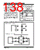
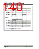
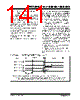
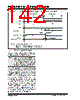
138 / 294 page  PIC16F631/677/685/687/689/690 DS41262D-page 136 © 2007 Microchip Technology Inc. 11.4.1 HALF-BRIDGE MODE In Half-Bridge mode, two pins are used as outputs to drive push-pull loads. The PWM output signal is output on the CCP1/P1A pin, while the complementary PWM output signal is output on the P1B pin (see Figure 11-6). This mode can be used for Half-Bridge applications, as shown in Figure 11-9, or for Full-Bridge applications, where four power switches are being modulated with two PWM signals. In Half-Bridge mode, the programmable dead-band delay can be used to prevent shoot-through current in Half-Bridge power devices. The value of the PDC<6:0> bits of the PWM1CON register sets the number of instruction cycles before the output is driven active. If the value is greater than the duty cycle, the corresponding output remains inactive during the entire cycle. See Section 11.4.6 “Programmable Dead-Band Delay mode” for more details of the dead-band delay operations. Since the P1A and P1B outputs are multiplexed with the PORT data latches, the associated TRIS bits must be cleared to configure P1A and P1B as outputs. FIGURE 11-8: EXAMPLE OF HALF-BRIDGE PWM OUTPUT FIGURE 11-9: EXAMPLE OF HALF-BRIDGE APPLICATIONS Period Pulse Width td td (1) P1A(2) P1B(2) td = Dead-Band Delay Period (1) (1) Note 1: At this time, the TMR2 register is equal to the PR2 register. 2: Output signals are shown as active-high. P1A P1B FET Driver FET Driver Load + - + - FET Driver FET Driver V+ Load FET Driver FET Driver P1A P1B Standard Half-Bridge Circuit (“Push-Pull”) Half-Bridge Output Driving a Full-Bridge Circuit |
|
ссылки URL |
| Вашему бизинису помогли Аллдатащит? [ DONATE ] |
Что такое Аллдатащит | реклама | контакт | Конфиденциальность | Ссылка на техническое описание | обмен ссыками | поиск по производителю All Rights Reserved©Alldatasheet.com |
| Russian : Alldatasheetru.com | Korean : Alldatasheet.co.kr | Spanish : Alldatasheet.es | French : Alldatasheet.fr | Italian : Alldatasheetit.com Portuguese : Alldatasheetpt.com | Polish : Alldatasheet.pl | Vietnamese : Alldatasheet.vn Indian : Alldatasheet.in | Mexican : Alldatasheet.com.mx | British : Alldatasheet.co.uk | New Zealand : Alldatasheet.co.nz |
|
Family Site : ic2ic.com |
icmetro.com |
 Russian ▼
 English
 Chinese
 German
 Japanese
 Russian
 Korean
 Spanish
 French
 Italian
 Portuguese
 Polish
 Vietnamese
 Indian
 Mexican
 British
 New Zealand