|
поискавой системы для электроныых деталей |
|
|
поискавой системы для электроныых деталей |
|
PIC16F631 датащи(PDF) 104 Page - Microchip Technology |
|
|
|||||||||||||||||||||||||||||
PIC16F631 датащи(HTML) 104 Page - Microchip Technology |
|
|
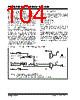
104 / 294 page  PIC16F631/677/685/687/689/690 DS41262D-page 102 © 2007 Microchip Technology Inc. 8.9 Comparator SR Latch The SR Latch module provides additional control of the comparator outputs. The module consists of a single SR latch and output multiplexers. The SR latch can be set, reset or toggled by the comparator outputs. The SR latch may also be set or reset, independent of comparator output, by control bits in the SRCON control register. The SR latch output multiplexers select whether the latch outputs or the comparator outputs are directed to the I/O port logic for eventual output to a pin. 8.9.1 LATCH OPERATION The latch is a Set-Reset latch that does not depend on a clock source. Each of the Set and Reset inputs are active-high. Each latch input is connected to a comparator output and a software controlled pulse generator. The latch can be set by C1OUT or the PULSS bit of the SRCON register. The latch can be reset by C2OUT or the PULSR bit of the SRCON register. The latch is reset-dominant, therefore, if both Set and Reset inputs are high, the latch will go to the Reset state. Both the PULSS and PULSR bits are self resetting which means that a single write to either of the bits is all that is necessary to complete a latch set or reset operation. 8.9.2 LATCH OUTPUT The SR<1:0> bits of the SRCON register control the latch output multiplexers and determine four possible output configurations. In these four configurations, the CxOUT I/O port logic is connected to: • C1OUT and C2OUT • C1OUT and SR latch Q • C2OUT and SR latch Q • SR latch Q and Q After any Reset, the default output configuration is the unlatched C1OUT and C2OUT mode. This maintains compatibility with devices that do not have the SR latch feature. The applicable TRIS bits of the corresponding ports must be cleared to enable the port pin output drivers. Additionally, the CxOE comparator output enable bits of the CMxCON0 registers must be set in order to make the comparator or latch outputs available on the output pins. The latch configuration enable states are completely independent of the enable states for the comparators. FIGURE 8-7: SR LATCH SIMPLIFIED BLOCK DIAGRAM C1SEN SR0 PULSS S R Q Q C2REN PULSR SR1 Note 1: If R = 1 and S = 1 simultaneously, Q = 0, Q = 1 2: Pulse generator causes a 1/2 Q-state (1 Tosc) pulse width. 3: Output shown for reference only. See I/O port pin block diagram for more detail. Pulse Gen(2) Pulse Gen(2) SYNCC2OUT (from comparator) C1OUT (from comparator) C2OE C2OUT pin(3) C1OE C1OUT pin(3) 0 1 MUX 1 0 MUX SR Latch(1) |
|
ссылки URL |
| Вашему бизинису помогли Аллдатащит? [ DONATE ] |
Что такое Аллдатащит | реклама | контакт | Конфиденциальность | Ссылка на техническое описание | обмен ссыками | поиск по производителю All Rights Reserved©Alldatasheet.com |
| Russian : Alldatasheetru.com | Korean : Alldatasheet.co.kr | Spanish : Alldatasheet.es | French : Alldatasheet.fr | Italian : Alldatasheetit.com Portuguese : Alldatasheetpt.com | Polish : Alldatasheet.pl | Vietnamese : Alldatasheet.vn Indian : Alldatasheet.in | Mexican : Alldatasheet.com.mx | British : Alldatasheet.co.uk | New Zealand : Alldatasheet.co.nz |
|
Family Site : ic2ic.com |
icmetro.com |
 Russian ▼
 English
 Chinese
 German
 Japanese
 Russian
 Korean
 Spanish
 French
 Italian
 Portuguese
 Polish
 Vietnamese
 Indian
 Mexican
 British
 New Zealand