|
поискавой системы для электроныых деталей |
|
|
поискавой системы для электроныых деталей |
|
PIC16F631 датащи(PDF) 103 Page - Microchip Technology |
|
|
|||||||||||||||||||||||||||||
PIC16F631 датащи(HTML) 103 Page - Microchip Technology |
|
|
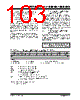
103 / 294 page  © 2007 Microchip Technology Inc. DS41262D-page 101 PIC16F631/677/685/687/689/690 8.8 Additional Comparator Features There are three additional comparator features: • Timer1 count enable (gate) • Synchronizing output with Timer1 • Simultaneous read of comparator outputs 8.8.1 COMPARATOR C2 GATING TIMER1 This feature can be used to time the duration or interval of analog events. Clearing the T1GSS bit of the CM2CON1 register will enable Timer1 to increment based on the output of Comparator C2. This requires that Timer1 is on and gating is enabled. See Section 6.0 “Timer1 Module with Gate Control” for details. It is recommended to synchronize the comparator with Timer1 by setting the C2SYNC bit when the comparator is used as the Timer1 gate source. This ensures Timer1 does not miss an increment if the comparator changes during an increment. 8.8.2 SYNCHRONIZING COMPARATOR C2 OUTPUT TO TIMER1 The Comparator C2 output can be synchronized with Timer1 by setting the C2SYNC bit of the CM2CON1 register. When enabled, the C2 output is latched on the falling edge of the Timer1 clock source. If a prescaler is used with Timer1, the comparator output is latched after the prescaling function. To prevent a race condition, the comparator output is latched on the falling edge of the Timer1 clock source and Timer1 increments on the rising edge of its clock source. See the Comparator Block Diagram (Figure 8-3) and the Timer1 Block Diagram (Figure 6-1) for more information. 8.8.3 SIMULTANEOUS COMPARATOR OUTPUT READ The MC1OUT and MC2OUT bits of the CM2CON1 register are mirror copies of both comparator outputs. The ability to read both outputs simultaneously from a single register eliminates the timing skew of reading separate registers. Note 1: Obtaining the status of C1OUT or C2OUT by reading CM2CON1 does not affect the comparator interrupt mismatch registers. REGISTER 8-3: CM2CON1: COMPARATOR C2 CONTROL REGISTER 1 R-0 R-0 U-0 U-0 U-0 U-0 R/W-1 R/W-0 MC1OUT MC2OUT — — — — T1GSS C2SYNC bit 7 bit 0 Legend: R = Readable bit W = Writable bit U = Unimplemented bit, read as ‘0’ -n = Value at POR ‘1’ = Bit is set ‘0’ = Bit is cleared x = Bit is unknown bit 7 MC1OUT: Mirror Copy of C1OUT bit bit 6 MC2OUT: Mirror Copy of C2OUT bit bit 5-2 Unimplemented: Read as ‘0’ bit 1 T1GSS: Timer1 Gate Source Select bit(1) 1 = Timer1 gate source is T1G 0 = Timer1 gate source is SYNCC2OUT. bit 0 C2SYNC: Comparator C2 Output Synchronization bit(2) 1 = Output is synchronous to falling edge of Timer1 clock 0 = Output is asynchronous Note 1: Refer to Section 6.6 “Timer1 Gate”. 2: Refer to Figure 8-3. |
|
ссылки URL |
| Вашему бизинису помогли Аллдатащит? [ DONATE ] |
Что такое Аллдатащит | реклама | контакт | Конфиденциальность | Ссылка на техническое описание | обмен ссыками | поиск по производителю All Rights Reserved©Alldatasheet.com |
| Russian : Alldatasheetru.com | Korean : Alldatasheet.co.kr | Spanish : Alldatasheet.es | French : Alldatasheet.fr | Italian : Alldatasheetit.com Portuguese : Alldatasheetpt.com | Polish : Alldatasheet.pl | Vietnamese : Alldatasheet.vn Indian : Alldatasheet.in | Mexican : Alldatasheet.com.mx | British : Alldatasheet.co.uk | New Zealand : Alldatasheet.co.nz |
|
Family Site : ic2ic.com |
icmetro.com |
 Russian ▼
 English
 Chinese
 German
 Japanese
 Russian
 Korean
 Spanish
 French
 Italian
 Portuguese
 Polish
 Vietnamese
 Indian
 Mexican
 British
 New Zealand