|
поискавой системы для электроныых деталей |
|
|
поискавой системы для электроныых деталей |
|
AD8231ACPZ-R7 датащи(PDF) 15 Page - Analog Devices |
|
|
|||||||||||||||||||||||||||||
AD8231ACPZ-R7 датащи(HTML) 15 Page - Analog Devices |
|
|
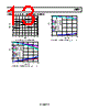
15 / 20 page  AD8231 Rev. 0 | Page 15 of 20 INCORRECT AD8231 IN-AMP VREF CORRECT AD8231 IN-AMP VREF AD8231 OP AMP + – Figure 31. Driving the Reference Pin LAYOUT The AD8231 is a high precision device. To ensure optimum performance at the PC board level, care must be taken in the design of the board layout. The AD8231 pinout is arranged in a logical manner to aid in this task. Power Supplies The AD8231 should be decoupled with a 0.1 μF bypass capacitor between the two supplies. This capacitor should be placed as close as possible to Pin 11 and Pin 12, either directly next to the pins or beneath the pins on the backside of the board. The AD8231’s auto- zero architecture requires a low ac impedance between the supplies. Long trace lengths to the bypass capacitor increase this impedance, which results in a larger input offset voltage. A stable dc voltage should be used to power the instrumentation amplifier. Noise on the supply pins can adversely affect performance. Package Considerations The AD8231 comes in a 4 mm × 4 mm LFCSP. Beware of blindly copying the footprint from another 4 mm × 4 mm LFCSP part; it may not have the same thermal pad size and leads. Refer to the Outline Dimensions section to verify that the PCB symbol has the correct dimensions. Space between the leads and thermal pad should be kept as wide as possible for the best bias current performance. Thermal Pad The AD8231 4 mm × 4 mm LFCSP comes with a thermal pad. This pad is connected internally to −VS. The pad can either be left unconnected or connected to the negative supply rail. For high vibration applications, a landing is recommended. Because the AD8231 dissipates little power, heat dissipation is rarely an issue. If improved heat dissipation is desired (for example, when ambient temperatures are near 125°C or when driving heavy loads), connect the thermal pad to the negative supply rail. For the best heat dissipation performance, the negative supply rail should be a plane in the board. See the Thermal Resistance section for thermal coefficients with and without the pad soldered. INPUT BIAS CURRENT RETURN PATH The input bias current of the AD8231 must have a return path to common. When the source, such as a thermocouple, cannot provide a return current path, one should be created, as shown in Figure 32. THERMOCOUPLE +VS REF –VS AD8231 CAPACITIVELY COUPLED +VS REF C C –VS AD8231 TRANSFORMER +VS REF –VS AD8231 INCORRECT CAPACITIVELY COUPLED +VS REF C R R C –VS AD8231 1 fHIGH-PASS = 2πRC THERMOCOUPLE +VS REF –VS 10MΩ AD8231 TRANSFORMER +VS REF –VS AD8231 CORRECT Figure 32. Creating an IBIAS Path RF INTERFERENCE RF rectification is often a problem when amplifiers are used in applications where there are strong RF signals. The disturbance can appear as a small dc offset voltage. High frequency signals can be filtered with a low-pass, RC network placed at the input of the instrumentation amplifier, as shown in Figure 33. The filter limits the input signal bandwidth according to the following relationship: ) (2 2 1 C D Diff C C R FilterFreq + π = C CM RC FilterFreq π = 2 1 where CD ≥ 10CC. |
|
|
ссылки URL |
| Вашему бизинису помогли Аллдатащит? [ DONATE ] |
Что такое Аллдатащит | реклама | контакт | Конфиденциальность | Ссылка на техническое описание | обмен ссыками | поиск по производителю All Rights Reserved©Alldatasheet.com |
| Russian : Alldatasheetru.com | Korean : Alldatasheet.co.kr | Spanish : Alldatasheet.es | French : Alldatasheet.fr | Italian : Alldatasheetit.com Portuguese : Alldatasheetpt.com | Polish : Alldatasheet.pl | Vietnamese : Alldatasheet.vn Indian : Alldatasheet.in | Mexican : Alldatasheet.com.mx | British : Alldatasheet.co.uk | New Zealand : Alldatasheet.co.nz |
|
Family Site : ic2ic.com |
icmetro.com |
 Russian ▼
 English
 Chinese
 German
 Japanese
 Russian
 Korean
 Spanish
 French
 Italian
 Portuguese
 Polish
 Vietnamese
 Indian
 Mexican
 British
 New Zealand