|
поискавой системы для электроныых деталей |
|
|
поискавой системы для электроныых деталей |
|
AD8231ACPZ-R7 датащи(PDF) 14 Page - Analog Devices |
|
|
|||||||||||||||||||||||||||||
AD8231ACPZ-R7 датащи(HTML) 14 Page - Analog Devices |
|
|
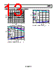
14 / 20 page  AD8231 Rev. 0 | Page 14 of 20 THEORY OF OPERATION –INB OUTB +INB OUTA –INA +INA REF –VS +VS CS A0 A1 A2 SDN AD8231 A1 A3 A4 14kΩ 14kΩ 14kΩ 14kΩ A2 Figure 30. Simplified Schematic AMPLIFIER ARCHITECTURE The AD8231 is based on the classic 3-op amp topology. This topology has two stages: a preamplifier to provide amplification, followed by a difference amplifier to remove the common-mode voltage. Figure 30 shows a simplified schematic of the AD8231. The preamp stage is composed of Amplifier A1, Amplifier A2, and a digitally controlled resistor network. The second stage is a gain of 1 difference amplifier composed of A3 and four 14 kΩ resistors. Amplifier A1, Amplifier A2, and Amplifier A3 are all zero drift, rail-to-rail input, rail-to rail-output amplifiers. The AD8231 design makes it extremely robust over tempera- ture. The AD8231 uses an internal thin film resistor to set the gain. Since all of the resistors are on the same die, gain temperature drift performance and CMRR drift performance are better than can be achieved with topologies using external resistors. The AD8231 also uses an auto-zero topology to null the offsets of all its internal amplifiers. Since this topology continually corrects for any offset errors, offset temperature drift is nearly nonexistent. The AD8231 also includes a free operational amplifier. Like the other amplifiers in the AD8231, it is a zero drift, rail-to-rail input, rail-to-rail output architecture. GAIN SELECTION The AD8231’s gain is set by voltages applied to the A0, A1, and A2 pins. To change the gain, the CS pin must be driven low. When the CS pin is driven high, the gain is latched, and voltages at the A0 to A2 pins have no effect. Table 7 shows the different gain settings. The time required for a gain change is dominated by the settling time of the amplifier. The AD8231 takes about 200 ns to switch gains, after which the amplifier begins to settle. Refer to Figure 16 through Figure 20 to determine the settling time for different gains. Table 7. Truth Table for AD8231 Gain Settings CS A2 A1 A0 Gain Low Low Low Low 1 Low Low Low High 2 Low Low High Low 4 Low Low High High 8 Low High Low Low 16 Low High Low High 32 Low High High Low 64 Low High High High 128 High X X X No change REFERENCE TERMINAL The output voltage of the AD8231 is developed with respect to the potential on the reference terminal. This is useful when the output signal needs to be offset to a midsupply level. For example, a voltage source can be tied to the REF pin to level- shift the output so that the AD8231 can drive a single-supply ADC. The REF pin is protected with ESD diodes and should not exceed either +VS or −VS by more than 0.3 V. For best performance, source impedance to the REF terminal should be kept below 1 Ω. As shown in Figure 30, the reference terminal, REF, is at one end of a 14 kΩ resistor. Additional impedance at the REF terminal adds to this 14 kΩ resistor and results in amplification of the signal connected to the positive input, causing a CMRR error. |
|
|
ссылки URL |
| Вашему бизинису помогли Аллдатащит? [ DONATE ] |
Что такое Аллдатащит | реклама | контакт | Конфиденциальность | Ссылка на техническое описание | обмен ссыками | поиск по производителю All Rights Reserved©Alldatasheet.com |
| Russian : Alldatasheetru.com | Korean : Alldatasheet.co.kr | Spanish : Alldatasheet.es | French : Alldatasheet.fr | Italian : Alldatasheetit.com Portuguese : Alldatasheetpt.com | Polish : Alldatasheet.pl | Vietnamese : Alldatasheet.vn Indian : Alldatasheet.in | Mexican : Alldatasheet.com.mx | British : Alldatasheet.co.uk | New Zealand : Alldatasheet.co.nz |
|
Family Site : ic2ic.com |
icmetro.com |
 Russian ▼
 English
 Chinese
 German
 Japanese
 Russian
 Korean
 Spanish
 French
 Italian
 Portuguese
 Polish
 Vietnamese
 Indian
 Mexican
 British
 New Zealand