|
поискавой системы для электроныых деталей |
|
|
поискавой системы для электроныых деталей |
|
34716 датащи(PDF) 14 Page - Freescale Semiconductor, Inc |
|
|
|||||||||||||||||||||||||||||
34716 датащи(HTML) 14 Page - Freescale Semiconductor, Inc |
|
|
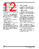
14 / 25 page  Analog Integrated Circuit Device Data 14 Freescale Semiconductor 34716 FUNCTIONAL DESCRIPTION FUNCTIONAL INTERNAL BLOCK DESCRIPTION TRACKING AND SEQUENCING This block allows the output of channel 2 of the 34716 to track 1/2 the voltage applied at the VREFIN pin. This allows the VREF and VTT voltages to track 1/2 VDDQ and assures that none of them will be higher than VDDQ at any point during normal operating conditions. For power down during a shutdown (S5) mode, the 34716 uses internal discharge MOSFETs (M8, M9, and M10 on Figure 2, page 2) to discharge VDDQ, VTT, and VREF respectively. These discharge MOSFETs are only active during shutdown mode. Using this block along with controlling the SD and STBY pins can offer the user the device for power sequencing by controlling when to turn the 34716 outputs on or off. BUCK CONVERTER This block provides the main function of the 34716: DC to DC conversion from an un-regulated input voltage to a regulated output voltage used by the loads for reliable operation. The buck converter is a high performance, fixed frequency (externally adjustable), Syncronous buck PWM voltage-mode control with a minimum on time of 100ns. It drives integrated 50 m Ω N-channel power MOSFETs saving board space and enhancing efficiency. The switching regulator output voltage is adjustable with an accuracy of less than ±2 % to meet DDR requirements. The regulator's voltage control loop is compensated using a type III compensation network, with external components to allow for optimizing the loop compensation, for a wide range of operating conditions. A typical Bootstrap circuit with an internal PMOS switch is used to provide the voltage necessary to properly enhance the high-side MOSFET gate. The 34716 is designed to address DDR memory power supplies. The integrated converter has the ability to supply up to 5.0 A out of channel 1 and sink and source up to 3.0 A of continuous current from channel 2, providing a full power supply solution for DDR applications. |
|
|
ссылки URL |
| Вашему бизинису помогли Аллдатащит? [ DONATE ] |
Что такое Аллдатащит | реклама | контакт | Конфиденциальность | Ссылка на техническое описание | обмен ссыками | поиск по производителю All Rights Reserved©Alldatasheet.com |
| Russian : Alldatasheetru.com | Korean : Alldatasheet.co.kr | Spanish : Alldatasheet.es | French : Alldatasheet.fr | Italian : Alldatasheetit.com Portuguese : Alldatasheetpt.com | Polish : Alldatasheet.pl | Vietnamese : Alldatasheet.vn Indian : Alldatasheet.in | Mexican : Alldatasheet.com.mx | British : Alldatasheet.co.uk | New Zealand : Alldatasheet.co.nz |
|
Family Site : ic2ic.com |
icmetro.com |
 Russian ▼
 English
 Chinese
 German
 Japanese
 Russian
 Korean
 Spanish
 French
 Italian
 Portuguese
 Polish
 Vietnamese
 Indian
 Mexican
 British
 New Zealand