|
поискавой системы для электроныых деталей |
|
|
поискавой системы для электроныых деталей |
|
34716 датащи(PDF) 12 Page - Freescale Semiconductor, Inc |
|
|
|||||||||||||||||||||||||||||
34716 датащи(HTML) 12 Page - Freescale Semiconductor, Inc |
|
|
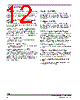
12 / 25 page  Analog Integrated Circuit Device Data 12 Freescale Semiconductor 34716 FUNCTIONAL DESCRIPTION FUNCTIONAL PIN DESCRIPTION ERROR AMPLIFIER INVERTING INPUT (INV1, INV2) Buck converter error amplifier inverting input. Connect the VDDQ voltage (channel 1) to INV1 pin through a resistor divider and connect the VTT voltage (channel 2) directly to INV2 pin. OUTPUT VOLTAGE DISCHARGE PATH (VOUT1, VOUT2) Buck converters output voltage are connected to these pins. It only serves as the output discharge path once the SD signal is asserted. INTERNAL SUPPLY VOLTAGE OUTPUT (VDDI) This is the output of the internal bias voltage regulator. Connect a 1.0 µF, 6 V low ESR ceramic filter capacitor between this pin and the GND pin. Filtering any spikes on this output is essential to the internal circuitry stable operation. SIGNAL GROUND (GND) Analog ground of the IC. Internal analog signals are referenced to this pin voltage. INPUT SUPPLY VOLTAGE (VIN) IC power supply input voltage. Input filtering is required for the device to operate properly. POWER GOOD OUTPUT SIGNAL (PG) This is an active low open drain output that is used to report the status of the device to a host. This output activates after a successful power up sequence and stays active as long as the device is in normal operation and is not experiencing any faults. This output activates after a 10 ms delay and must be pulled up by an external resistor to a supply voltage like VIN. STANDBY INPUT (STBY) If this pin is tied to the GND pin, the device will be in Standby Mode. If left unconnected or tied to the VIN pin, the device will be in Normal Mode. The pin has an internal pull up of 1.5 M Ω. This input accepts the S3 (Suspend-To-RAM) control signal. SHUTDOWN INPUT (SD) If this pin is tied to the GND pin, the device will be in Shutdown Mode. If left unconnected or tied to the VIN pin, the device will be in Normal Mode. The pin has an internal pull up of 1.5 M Ω. This input accepts the S5 (Suspend-To-Disk) control signal. REFERENCE VOLTAGE OUTPUT (VREFOUT) This is a buffered reference voltage output that is equal to 1/2 VREFIN. It has a 10.0 mA current drive capability. This output is used as the VREF voltage rail and should be filtered against any noise. Connect a 0.1 µF, 6 V low ESR ceramic filter capacitor between this pin and the GND pin and between this pin and VDDQ rail. VREFOUT is also used as the reference voltage for the buck converter error amplifier. REFERENCE VOLTAGE INPUT (VREFIN) The output of channel two will track 1/2 the voltage applied at this pin. FREQUENCY ADJUSTMENT INPUT (FREQ) The buck converters switching frequency can be adjusted by connecting this pin to an external resistor divider between VDDI and GND pins. The default switching frequency (FREQ pin connected to ground, GND) is set at 1.0 MHz. CHANNEL 1 SOFT START ADJUSTMENT INPUT (ILIM1) Channel one Soft Start can be adjusted by applying a voltage between 1.25V and VDDI. |
|
|
ссылки URL |
| Вашему бизинису помогли Аллдатащит? [ DONATE ] |
Что такое Аллдатащит | реклама | контакт | Конфиденциальность | Ссылка на техническое описание | обмен ссыками | поиск по производителю All Rights Reserved©Alldatasheet.com |
| Russian : Alldatasheetru.com | Korean : Alldatasheet.co.kr | Spanish : Alldatasheet.es | French : Alldatasheet.fr | Italian : Alldatasheetit.com Portuguese : Alldatasheetpt.com | Polish : Alldatasheet.pl | Vietnamese : Alldatasheet.vn Indian : Alldatasheet.in | Mexican : Alldatasheet.com.mx | British : Alldatasheet.co.uk | New Zealand : Alldatasheet.co.nz |
|
Family Site : ic2ic.com |
icmetro.com |
 Russian ▼
 English
 Chinese
 German
 Japanese
 Russian
 Korean
 Spanish
 French
 Italian
 Portuguese
 Polish
 Vietnamese
 Indian
 Mexican
 British
 New Zealand