|
поискавой системы для электроныых деталей |
|
|
поискавой системы для электроныых деталей |
|
ADIN1300BCPZ-R7 датащи(PDF) 66 Page - Analog Devices |
|
|
|||||||||||||||||||||||||||||
ADIN1300BCPZ-R7 датащи(HTML) 66 Page - Analog Devices |
|
|
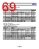
66 / 79 page  ADIN1300 Data Sheet Rev. 0 | Page 66 of 79 Start of Packet Receive Detection Delay Register Address: 0x9429, Reset: 0x0000, Name: SOP_RX_DEL This register controls the receive side SOP detection delay. Table 95. Bit Descriptions for SOP_RX_DEL Bits Bit Name Description Reset Access [15:11] SOP_RX_10_DEL_NCYC This bit field specifies the number of cycles of the MII RX_CLK clock to delay the received frames SOP indication for 10BASE-T links. 0x0 R/W [10:6] SOP_RX_100_DEL_NCYC This bit field specifies the number of cycles of the MII RX_CLK clock to delay the received frames SOP indication for 100BASE-TX links. 0x0 R/W [5:0] SOP_RX_1000_DEL_NCYC This register field specifies the number of cycles of the receive clock (for example, 8 ns cycles) to delay the received frames SOP indication for 1000BASE-T links. It is mainly intended to support MAC interfaces with long latency in Gigabit mode (like SGMII) so that the received frame SOP indication is not asserted before the MAC receives the frame. 0x0 R/W Start of Packet Transmit Detection Delay Register Address: 0x942A, Reset: 0x0000, Name: SOP_TX_DEL This register controls the transmit side SOP detection delay. Table 96. Bit Descriptions for SOP_TX_DEL Bits Bit Name Description Reset Access [15:13] RESERVED Reserved. 0x0 R [12:8] SOP_TX_10_DEL_N_8_NS This bit field specifies the number of 8 ns periods to delay the transmitted frames SOP indication for 10BASE-T links. To align the transmit SOP indication assertion close to the reference point set on the MDI pins, set this register to 5'd20. 0x0 R/W [7:4] SOP_TX_100_DEL_N_8_NS This bit field specifies the number of 8 ns periods to delay the transmitted frames SOP indication for 100BASE-TX links. To align the transmit SOP indication assertion close to the reference point set on the MDI pins, set this register to 4'd0. 0x0 R/W [3:0] SOP_TX_1000_DEL_N_8_NS This bit field specifies the number of 8 ns periods to delay the transmitted frames SOP indication for 1000BASE-T links. To align the transmit SOP indication assertion close to the reference point set on the MDI pins (so that the timestamping point does not have to be adjusted at the MAC/switch side), set this register to 4'd6. 0x0 R/W Control of FIFO Depth for MII Modes Register Address: 0x9602, Reset: 0x0001, Name: DPTH_MII_BYTE FIFO depth in bytes in MII modes. Table 97. Bit Descriptions for DPTH_MII_BYTE Bits Bit Name Description Reset Access [15:1] RESERVED Reserved. 0x0 R 0 DPTH_MII_BYTE Applies to MII modes for 10 Mbps and 100 Mbps. When set, the FIFO depth is in bytes. When zero, the FIFO depth is in nibbles. The default value of this bit is 1. Therefore, the FIFO prefill is set in bytes. In MII mode, because the interface is nibble based, the internal prefill in the transmit FIFO is larger and, therefore, the latency is longer. 0x1 R/W |
|
ссылки URL |
| Вашему бизинису помогли Аллдатащит? [ DONATE ] |
Что такое Аллдатащит | реклама | контакт | Конфиденциальность | Ссылка на техническое описание | обмен ссыками | поиск по производителю All Rights Reserved©Alldatasheet.com |
| Russian : Alldatasheetru.com | Korean : Alldatasheet.co.kr | Spanish : Alldatasheet.es | French : Alldatasheet.fr | Italian : Alldatasheetit.com Portuguese : Alldatasheetpt.com | Polish : Alldatasheet.pl | Vietnamese : Alldatasheet.vn Indian : Alldatasheet.in | Mexican : Alldatasheet.com.mx | British : Alldatasheet.co.uk | New Zealand : Alldatasheet.co.nz |
|
Family Site : ic2ic.com |
icmetro.com |
 Russian ▼
 English
 Chinese
 German
 Japanese
 Russian
 Korean
 Spanish
 French
 Italian
 Portuguese
 Polish
 Vietnamese
 Indian
 Mexican
 British
 New Zealand