|
поискавой системы для электроныых деталей |
|
|
поискавой системы для электроныых деталей |
|
LTC2611CDD датащи(PDF) 12 Page - Linear Technology |
|
|
|||||||||||||||||||||||||||||
LTC2611CDD датащи(HTML) 12 Page - Linear Technology |
|
|
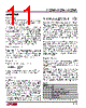
12 / 16 page  12 LTC2601/LTC2611/LTC2621 2601f OPERATIO INPUT WORD (LTC2601) Because of this, the devices can be addressed and con- trolled individually by simply concatenating their input words; the first instruction addresses the last device in the chain and so forth. The SCK and CS/LD signals are common to all devices in the series. In use, CS/LD is first taken low. Then the concatenated input data is transferred to the chain, using SDI of the first device as the data input. When the data transfer is com- plete, CS/LD is taken high, which executes the commands specified for each of the devices simultaneously. A single device can be controlled by using the no-operation com- mand (1111) for the other devices in the chain. Power-Down Mode For power-constrained applications, power-down mode can be used to reduce the supply current whenever the DAC output is not needed. When in power-down, the buffer amplifier, bias circuit and reference input is dis- abled and draws essentially zero current. The DAC output is put into a high impedance state, and the output pin is passively pulled to ground through 90k resistors. Input- and DAC-register contents are not disturbed during power- down. The DAC can be put into power-down mode by using command 0100b. The 16-bit data word is ignored. The supply and reference currents are reduced to almost zero when the DAC is powered down; the effective resistance at REF rises accordingly becoming a high impedance input (typically > 1G Ω). Normal operation can be resumed by executing any com- mand which includes a DAC update, as shown in Table 1 or performing an asynchronous update (LDAC) as de- scribed in the next section. The DAC is powered up as its voltage output is updated. When the DAC in powered- down state is powered up and updated, normal settling is delayed. The main bias generation circuit block has been automatically shut down in addition to the DAC amplifier and reference input and so the power up delay time is 12 µs (for VCC = 5V) or 30µs (for VCC = 3V). Asynchronous DAC Update Using LDAC In addition to the update commands shown in Table 1, the LDAC pin asynchronously updates the DAC register with the contents of the input register. If CS/LD is high, a low on the LDAC pin causes the DAC register to be updated with the contents of the input register. If CS/LD is low, a low going pulse on the LDAC pin before the rising edge of CS/LD powers up the DAC but does not cause the output to be updated. If LDAC remains low after the rising edge of CS/LD, then LDAC is recognized, the command specified in the 24-bit word just transferred is executed and the DAC output is updated. INPUT WORD (LTC2611) INPUT WORD (LTC2621) C3 COMMAND DON’T CARE BITS DATA (16 BITS) C2 C1 C0 X X X X D13 D14 D15 D12 D11 D10 D9 D8 D7 D6 D5 D4 D3 D2 D1 D0 2601 TBL01 MSB LSB C3 COMMAND DON’T CARE BITS DATA (14 BITS + 2 DON’T CARE BITS) C2 C1 C0 X X X X D13 D12 D11 D10 D9 D8 D7 D6 D5 D4 D3 D2 D1 D0 X X 2601 TBL02 MSB LSB C3 COMMAND DON’T CARE BITS DATA (12 BITS + 4 DON’T CARE BITS) C2 C1 C0 X X X X D11 D10 D9 D8 D7 D6 D5 D4 D3 D2 D1 D0 X X XX 2601 TBL03 MSB LSB |
|
|
ссылки URL |
| Вашему бизинису помогли Аллдатащит? [ DONATE ] |
Что такое Аллдатащит | реклама | контакт | Конфиденциальность | Ссылка на техническое описание | обмен ссыками | поиск по производителю All Rights Reserved©Alldatasheet.com |
| Russian : Alldatasheetru.com | Korean : Alldatasheet.co.kr | Spanish : Alldatasheet.es | French : Alldatasheet.fr | Italian : Alldatasheetit.com Portuguese : Alldatasheetpt.com | Polish : Alldatasheet.pl | Vietnamese : Alldatasheet.vn Indian : Alldatasheet.in | Mexican : Alldatasheet.com.mx | British : Alldatasheet.co.uk | New Zealand : Alldatasheet.co.nz |
|
Family Site : ic2ic.com |
icmetro.com |
 Russian ▼
 English
 Chinese
 German
 Japanese
 Russian
 Korean
 Spanish
 French
 Italian
 Portuguese
 Polish
 Vietnamese
 Indian
 Mexican
 British
 New Zealand