|
поискавой системы для электроныых деталей |
|
|
поискавой системы для электроныых деталей |
|
LTC2611CDD датащи(PDF) 11 Page - Linear Technology |
|
|
|||||||||||||||||||||||||||||
LTC2611CDD датащи(HTML) 11 Page - Linear Technology |
|
|
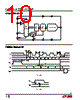
11 / 16 page  11 LTC2601/LTC2611/LTC2621 2601f Table 1. COMMAND* C3 C2 C1 C0 0000 Write to Input Register 0001 Update (Power Up) DAC Register 0011 Write to and Update (Power Up) 0100 Power Down 1111 No Operation *Command codes not shown are reserved and should not be used. device to execute the command specified in the 24-bit input word. The complete sequence is shown in Figure 2a. The command (C3-C0) assignments are shown in Table 1. The first four commands in the table consist of write and update operations. A write operation loads a 16-bit data word from the 32-bit shift register into the input register of the DAC. In an update operation, the data word is copied from the input register to the DAC register and converted to an analog voltage at the DAC output. The update operation also powers up the DAC if it had been in power- down mode. The data path and registers are shown in the Block Diagram. While the minimum input word is 24 bits, it may optionally be extended to 32 bits. To use the 32-bit word width, 8 don’t-care bits are transferred to the device first, fol- lowed by the 24-bit word as just described. Figure 2b shows the 32-bit sequence. The 32-bit word is required for daisy-chain operation, and is also available to accommo- date microprocessors which have a minimum word width of 16 bits (2 bytes). Daisy-Chain Operation The serial output of the shift register appears at the SDO pin. Data transferred to the device from the SDI input is delayed 32 SCK rising edges before being output at the next SCK falling edge. The SDO output can be used to facilitate control of multiple serial devices from a single 3-wire serial port (i.e., SCK, SDI and CS/LD). Such a “daisy chain” series is configured by connecting SDO of each upstream device to SDI of the next device in the chain. The shift registers of the devices are thus connected in series, effectively forming a single input shift register which extends through the entire chain. OPERATIO Power-On Reset The LTC2601/LTC2611/LTC2621 clear the outputs to zero scale when power is first applied, making system initializa- tion consistent and repeatable. For some applications, downstream circuits are active during DAC power-up, and may be sensitive to nonzero outputs from the DAC during this time. The LTC2601/ LTC2611/LTC2621 contain circuitry to reduce the power- on glitch; furthermore, the glitch amplitude can be made arbitrarily small by reducing the ramp rate of the power supply. For example, if the power supply is ramped to 5V in 1ms, the analog outputs rise less than 10mV above ground (typ) during power-on. See Power-On Reset Glitch in the Typical Performance Characteristics section. Power Supply Sequencing The voltage at REF (Pin 6) should be kept within the range – 0.3V ≤ VREF ≤ VCC + 0.3V (see Absolute Maximum Ratings). Particular care should be taken to observe these limits during power supply turn-on and turn-off sequences, when the voltage at VCC (Pin 16) is in transition. Transfer Function The digital-to-analog transfer function is: V k V OUT IDEAL N REF () = 2 where k is the decimal equivalent of the binary DAC input code, N is the resolution and VREF is the voltage at REF (Pin 6). Serial Interface The CS/LD input is level triggered. When this input is taken low, it acts as a chip-select signal, powering-on the SDI and SCK buffers and enabling the input shift register. Data (SDI input) is transferred at the next 24 rising SCK edges. The 4-bit command, C3-C0, is loaded first; then 4 don’t care bits; and finally the 16-bit data word. The data word comprises the 16-, 14- or 12-bit input code, ordered MSB- to-LSB, followed by 0, 2 or 4 don’t care bits (LTC2601, LTC2611 and LTC2621 respectively). Data can only be transferred to the device when the CS/LD signal is low.The rising edge of CS/LD ends the data transfer and causes the |
|
|
ссылки URL |
| Вашему бизинису помогли Аллдатащит? [ DONATE ] |
Что такое Аллдатащит | реклама | контакт | Конфиденциальность | Ссылка на техническое описание | обмен ссыками | поиск по производителю All Rights Reserved©Alldatasheet.com |
| Russian : Alldatasheetru.com | Korean : Alldatasheet.co.kr | Spanish : Alldatasheet.es | French : Alldatasheet.fr | Italian : Alldatasheetit.com Portuguese : Alldatasheetpt.com | Polish : Alldatasheet.pl | Vietnamese : Alldatasheet.vn Indian : Alldatasheet.in | Mexican : Alldatasheet.com.mx | British : Alldatasheet.co.uk | New Zealand : Alldatasheet.co.nz |
|
Family Site : ic2ic.com |
icmetro.com |
 Russian ▼
 English
 Chinese
 German
 Japanese
 Russian
 Korean
 Spanish
 French
 Italian
 Portuguese
 Polish
 Vietnamese
 Indian
 Mexican
 British
 New Zealand