|
поискавой системы для электроныых деталей |
|
|
поискавой системы для электроныых деталей |
|
LTC2611CDD датащи(PDF) 9 Page - Linear Technology |
|
|
|||||||||||||||||||||||||||||
LTC2611CDD датащи(HTML) 9 Page - Linear Technology |
|
|
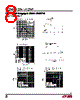
9 / 16 page  9 LTC2601/LTC2611/LTC2621 2601f PIN FUNCTIONS SDO (Pin 1): Serial Interface Data Output. The serial output of the shift register appears at the SDO pin. The data transferred to the device via the SDI pin is delayed 32 SCK rising edges before being output at the next falling edge. This pin is used for daisy-chain operation. SDI (Pin 2): Serial Interface Data Input. Data is applied to SDI for transfer to the device at the rising edge of SCK (Pin 3). The LTC2601 accepts input word lengths of either 24 or 32 bits. SCK (Pin 3): Serial Interface Clock Input. CMOS and TTL compatible. CLR (Pin 4): Asynchronous Clear Input. A logic low at this level-triggered input clears all registers and causes the DAC voltage outputs to drop to 0V. CMOS and TTL compatible. CS/LD (Pin 5): Serial Interface Chip Select/Load Input. When CS/LD is low, SCK is enabled for shifting data on SDI into the register. When CS/LD is taken high, SCK is disabled and the specified command (see Table 1) is executed. REF (Pin 6): Reference Voltage Input. 0V ≤ VREF ≤ VCC. VOUT (Pin 7): DAC Analog Voltage Output. The output range is 0V to VREF. GND (Pin 8): Analog Ground. VCC (Pin 9): Supply Voltage Input. 2.5V ≤ VCC ≤ 5.5V. LDAC (Pin 10): Asynchronous DAC Update Pin. If CS/LD is high, a falling edge on LDAC immediately updates the DAC register with the contents of the input register (simi- lar to a software update). If CS/LD is low when LDAC goes low, the DAC register is updated after CS/LD returns high. A low on the LDAC pin powers up the DAC. A software power down command is ignored if LDAC is low. Exposed Pad (Pin 11): Ground. Must be soldered to PCB ground. |
|
|
ссылки URL |
| Вашему бизинису помогли Аллдатащит? [ DONATE ] |
Что такое Аллдатащит | реклама | контакт | Конфиденциальность | Ссылка на техническое описание | обмен ссыками | поиск по производителю All Rights Reserved©Alldatasheet.com |
| Russian : Alldatasheetru.com | Korean : Alldatasheet.co.kr | Spanish : Alldatasheet.es | French : Alldatasheet.fr | Italian : Alldatasheetit.com Portuguese : Alldatasheetpt.com | Polish : Alldatasheet.pl | Vietnamese : Alldatasheet.vn Indian : Alldatasheet.in | Mexican : Alldatasheet.com.mx | British : Alldatasheet.co.uk | New Zealand : Alldatasheet.co.nz |
|
Family Site : ic2ic.com |
icmetro.com |
 Russian ▼
 English
 Chinese
 German
 Japanese
 Russian
 Korean
 Spanish
 French
 Italian
 Portuguese
 Polish
 Vietnamese
 Indian
 Mexican
 British
 New Zealand