|
поискавой системы для электроныых деталей |
|
|
поискавой системы для электроныых деталей |
|
AD7622BSTZ датащи(PDF) 21 Page - Analog Devices |
|
|
|||||||||||||||||||||||||||||
AD7622BSTZ датащи(HTML) 21 Page - Analog Devices |
|
|
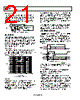
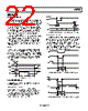
21 / 29 page  AD7622 Rev. 0 | Page 20 of 28 Temperature Sensor The TEMP pin measures the temperature of the AD7622. To improve the calibration accuracy over the temperature range, the output of the TEMP pin is applied to one of the inputs of the analog switch (such as, ADG779), and the ADC itself is used to measure its own temperature. This configuration is shown in Figure 29. ADG779 AD8021 CC ANALOG INPUT (UNIPOLAR) AD7622 IN+ TEMPERATURE SENSOR TEMP Figure 29. Use of the Temperature Sensor POWER SUPPLY The AD7622 uses three sets of power supply pins: an analog 2.5 V supply AVDD, a digital 2.5 V core supply DVDD, and a digital input/output interface supply OVDD. The OVDD supply allows direct interface with any logic working between 2.3 V and 5.25 V. To reduce the number of supplies needed, the digital core (DVDD) can be supplied through a simple RC filter from the analog supply, as shown in Figure 24. Power Sequencing The AD7622 is independent of power supply sequencing and thus free from supply induced voltage latch-up. In addition, it is very insensitive to power supply variations over a wide frequency range, as shown in Figure 30. 65.0 45.0 1 10000 FREQUENCY (kHz) 10 100 1000 47.5 50.0 52.5 55.0 57.5 60.0 62.5 EXT REF INT REF Figure 30. PSRR vs. Frequency Power-Up At power-up, or when returning to operational mode from the power-down mode (PD = high), the AD7622 engages an initialization process. During this time, the first 128 conversions should be ignored or the RESET input could be pulsed to engage a faster initialization process. Refer to the Digital Interface section for RESET and timing details. A simple power-on reset circuit, as shown in Figure 24, can be used to minimize the digital interface. As OVDD powers up, the capacitor is shorted and brings RESET high; it is then charged returning RESET to low. However, this circuit only works when powering up the AD7622 because the power-down mode (PD = high) does not power down any of the supplies and as a result, RESET is low. It should be noted that the digital interface remains active even during the acquisition phase. To reduce the operating digital supply currents even further, drive the digital inputs close to the power rails (that is, OVDD and OGND). CONVERSION CONTROL The AD7622 is controlled by the CNVST input. A falling edge on CNVST is all that is necessary to initiate a conversion. Detailed timing diagrams of the conversion process are shown in Figure 31. Once initiated, it cannot be restarted or aborted, even by the power-down input, PD, until the conversion is complete. The CNVST signal operates independently of CS and RD signals. BUSY MODE CONVERT ACQUIRE ACQUIRE CONVERT CNVST t1 t2 t4 t3 t5 t6 t7 t8 Figure 31. Basic Conversion Timing For optimal performance, the rising edge of CNVST should not occur after the maximum CNVST low time, t1, or until the end of conversion. Although CNVST is a digital signal, it should be designed with special care with fast, clean edges and levels with minimum overshoot and undershoot or ringing. The CNVST trace should be shielded with ground and a low value serial resistor (for example, 50 Ω) termination should be added close to the output of the component that drives this line. In addition, a 50 pF capacitor is recommended to further reduce the effects of overshoot and undershoot as shown in Figure 24. For applications where SNR is critical, the CNVST signal should have very low jitter. This can be achieved by using a dedicated oscillator for CNVST generation, or by clocking CNVST with a high frequency, low jitter clock, as shown in Figure 24. |
|
ссылки URL |
| Вашему бизинису помогли Аллдатащит? [ DONATE ] |
Что такое Аллдатащит | реклама | контакт | Конфиденциальность | Ссылка на техническое описание | обмен ссыками | поиск по производителю All Rights Reserved©Alldatasheet.com |
| Russian : Alldatasheetru.com | Korean : Alldatasheet.co.kr | Spanish : Alldatasheet.es | French : Alldatasheet.fr | Italian : Alldatasheetit.com Portuguese : Alldatasheetpt.com | Polish : Alldatasheet.pl | Vietnamese : Alldatasheet.vn Indian : Alldatasheet.in | Mexican : Alldatasheet.com.mx | British : Alldatasheet.co.uk | New Zealand : Alldatasheet.co.nz |
|
Family Site : ic2ic.com |
icmetro.com |
 Russian ▼
 English
 Chinese
 German
 Japanese
 Russian
 Korean
 Spanish
 French
 Italian
 Portuguese
 Polish
 Vietnamese
 Indian
 Mexican
 British
 New Zealand