|
поискавой системы для электроныых деталей |
|
|
поискавой системы для электроныых деталей |
|
ADRF5130BCPZ-R7 датащи(PDF) 8 Page - Analog Devices |
|
|
|||||||||||||||||||||||||||||
ADRF5130BCPZ-R7 датащи(HTML) 8 Page - Analog Devices |
|
|
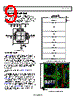
8 / 11 page  Data Sheet ADRF5130 Rev. A | Page 7 of 10 THEORY OF OPERATION The ADRF5130 requires a single-supply voltage applied to the VDD pin. Bypass capacitors are recommended on the supply line to minimize RF coupling. A digital control voltage applied to the VCTL pin controls the ADRF5130. A small bypassing capacitor is recommended on these digital signal lines to improve the RF signal isolation. The ADRF5130 is internally matched to 50 Ω at the RF input port (RFC) and the RF output ports (RF1 and RF2); therefore, no external matching components are required. The RFx pins are dc-coupled, and dc blocking capacitors are required on the RF lines. The design is bidirectional; the input and outputs are interchangeable. The ideal power-up sequence of the ADRF5130 is as follows: 1. Connect to GND. 2. Power up VDD. 3. Power up the digital control input. Powering the digital control input before the VDD supply can inadvertently forward-bias and damage the ESD protection structures. 4. Power up the RF input. Depending on the logic level applied to the VCTL pin, one RF output port (for example, RF1) is set to on mode, by which an insertion loss path is provided from the input to the output, while the other RF output port (for example, RF2) is set to off mode, by which the output is isolated from the input. Table 5. Switch Operation Mode Digital Control Input (VCTL) Switch Mode RFC to RF1 RFC to RF2 0 Off mode: the RF1 port is isolated from the RFC port and is internally terminated to a 50 Ω load to absorb the applied RF signals. On mode: a low insertion loss path from the RFC port to the RF2 port. 1 On mode: a low insertion loss path from the RFC port to the RF1 port. Off mode: the RF2 port is isolated from the RFC port and is internally terminated to a 50 Ω load to absorb the applied RF signals. |
|
|
ссылки URL |
| Вашему бизинису помогли Аллдатащит? [ DONATE ] |
Что такое Аллдатащит | реклама | контакт | Конфиденциальность | Ссылка на техническое описание | обмен ссыками | поиск по производителю All Rights Reserved©Alldatasheet.com |
| Russian : Alldatasheetru.com | Korean : Alldatasheet.co.kr | Spanish : Alldatasheet.es | French : Alldatasheet.fr | Italian : Alldatasheetit.com Portuguese : Alldatasheetpt.com | Polish : Alldatasheet.pl | Vietnamese : Alldatasheet.vn Indian : Alldatasheet.in | Mexican : Alldatasheet.com.mx | British : Alldatasheet.co.uk | New Zealand : Alldatasheet.co.nz |
|
Family Site : ic2ic.com |
icmetro.com |
 Russian ▼
 English
 Chinese
 German
 Japanese
 Russian
 Korean
 Spanish
 French
 Italian
 Portuguese
 Polish
 Vietnamese
 Indian
 Mexican
 British
 New Zealand