|
поискавой системы для электроныых деталей |
|
|
поискавой системы для электроныых деталей |
|
PIC16C71-04/SP датащи(PDF) 114 Page - Microchip Technology |
|
|
|||||||||||||||||||||||||||||
PIC16C71-04/SP датащи(HTML) 114 Page - Microchip Technology |
|
|
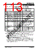
114 / 176 page  PIC16C71X DS30272A-page 114 © 1997 Microchip Technology Inc. Applicable Devices 710 71 711 715 13.2 DC Characteristics: PIC16LC715-04 (Commercial, Industrial) DC CHARACTERISTICS Standard Operating Conditions (unless otherwise stated) Operating temperature 0˚C ≤ TA ≤ +70˚C (commercial) -40˚C ≤ TA ≤ +85˚C (industrial) Param No. Characteristic Sym Min Typ† Max Units Conditions D001 Supply Voltage VDD 2.5 - 5.5 V LP, XT, RC osc configuration (DC - 4 MHz) D002* RAM Data Retention Voltage (Note 1) VDR - 1.5 - V Device in SLEEP mode D003 VDD start voltage to ensure internal Power-on Reset signal VPOR - VSS - V See section on Power-on Reset for details D004* VDD rise rate to ensure internal Power-on Reset signal SVDD 0.05 - - V/ms See section on Power-on Reset for details D005 Brown-out Reset Voltage BVDD 3.7 4.0 4.3 V BODEN configuration bit is enabled D010 D010A Supply Current (Note 2) IDD - - 2.0 22.5 3.8 48 mA µA XT, RC osc configuration FOSC = 4 MHz, VDD = 3.0V (Note 4) LP osc configuration FOSC = 32 kHz, VDD = 3.0V, WDT disabled D015 Brown-out Reset Current (Note 5) ∆IBOR - 300* 500 µA BOR enabled VDD = 5.0V D020 D021 D021A Power-down Current (Note 3) IPD - - - 7.5 0.9 0.9 30 5 5 µA µA µA VDD = 3.0V, WDT enabled, -40 °C to +85°C VDD = 3.0V, WDT disabled, 0 °C to +70°C VDD = 3.0V, WDT disabled, -40 °C to +85°C D023 Brown-out Reset Current (Note 5) ∆IBOR - 300* 500 µA BOR enabled VDD = 5.0V * These parameters are characterized but not tested. † Data in "Typ" column is at 5V, 25˚C unless otherwise stated. These parameters are for design guidance only and are not tested. Note 1: This is the limit to which VDD can be lowered in SLEEP mode without losing RAM data. 2: The supply current is mainly a function of the operating voltage and frequency. Other factors such as I/O pin loading and switching rate, oscillator type, internal code execution pattern, and temperature also have an impact on the current consumption. The test conditions for all IDD measurements in active operation mode are: OSC1 = external square wave, from rail to rail; all I/O pins tristated, pulled to VDD MCLR = VDD; WDT enabled/disabled as specified. 3: The power-down current in SLEEP mode does not depend on the oscillator type. Power-down current is measured with the part in SLEEP mode, with all I/O pins in hi-impedance state and tied to VDD and VSS. 4: For RC osc configuration, current through Rext is not included. The current through the resistor can be esti- mated by the formula Ir = VDD/2Rext (mA) with Rext in kOhm. 5: The ∆ current is the additional current consumed when this peripheral is enabled. This current should be added to the base IDD or IPD measurement. |
|
ссылки URL |
| Вашему бизинису помогли Аллдатащит? [ DONATE ] |
Что такое Аллдатащит | реклама | контакт | Конфиденциальность | Ссылка на техническое описание | обмен ссыками | поиск по производителю All Rights Reserved©Alldatasheet.com |
| Russian : Alldatasheetru.com | Korean : Alldatasheet.co.kr | Spanish : Alldatasheet.es | French : Alldatasheet.fr | Italian : Alldatasheetit.com Portuguese : Alldatasheetpt.com | Polish : Alldatasheet.pl | Vietnamese : Alldatasheet.vn Indian : Alldatasheet.in | Mexican : Alldatasheet.com.mx | British : Alldatasheet.co.uk | New Zealand : Alldatasheet.co.nz |
|
Family Site : ic2ic.com |
icmetro.com |
 Russian ▼
 English
 Chinese
 German
 Japanese
 Russian
 Korean
 Spanish
 French
 Italian
 Portuguese
 Polish
 Vietnamese
 Indian
 Mexican
 British
 New Zealand