|
поискавой системы для электроныых деталей |
|
|
поискавой системы для электроныых деталей |
|
LT1161 датащи(PDF) 6 Page - Linear Technology |
|
|
|||||||||||||||||||||||||||||
LT1161 датащи(HTML) 6 Page - Linear Technology |
|
|
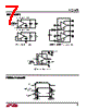
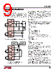
6 / 20 page  6 LTC1693 PIN FUNCTIONS SO-8 Package (LTC1693-1, LTC1693-2) IN1, IN2 (Pins 1, 3): Driver Inputs. The inputs have VCC independent thresholds with 1.2V typical hysteresis to improve noise immunity. GND1, GND2 (Pins 2, 4): Driver Grounds. Connect to a low impedance ground. The VCC bypass capacitor should connect directly to this pin. The source of the external MOSFET should also connect directly to the ground pin. This minimizes the AC current path and improves signal integrity. The ground pins should not be tied together if isolation is required between the two drivers of the LTC1693-1 and the LTC1693-2. OUT 1, OUT2 (Pins 5, 7): Driver Outputs. The LTC1693- 1’s outputs are in phase with their respective inputs (IN1, IN2). The LTC1693-2’s topside driver output (OUT1) is in phase with its input (IN1) and the bottom side driver’s output (OUT2) is opposite in phase with respect to its input pin (IN2). VCC1, VCC2 (Pins 6, 8): Power Supply Inputs. MSOP Package (LTC1693-3) IN (Pin 1): Driver Input. The input has VCC independent thresholds with hysteresis to improve noise immunity. NC (Pins 2, 5, 6): No Connect. PHASE (Pin 3): Output Polarity Select. Connect this pin to VCC or leave it floating for noninverting operation. Ground this pin for inverting operation. The typical PHASE pin input current when pulled low is 20 µA. GND (Pin 4): Driver Ground. Connect to a low impedance ground. The VCC bypass capacitor should connect directly to this pin. The source of the external MOSFET should also connect directly to the ground pin. This minimizes the AC current path and improves signal integrity. OUT (Pin 7): Driver Output. VCC (Pin 8): Power Supply Input. VCC1 8 LTC1693-1 DUAL NONINVERTING DRIVER 7 1 2 OUT1 IN1 GND1 VCC2 6 5 3 4 OUT2 IN2 GND2 VCC 8 LTC1693-3 SINGLE DRIVER WITH POLARITY SELECT 7 1 4 OUT IN GND NC 6 5 3 2 NC 1693 BD PHASE NC VCC1 8 LTC1693-2 TOPSIDE NONINVERTING DRIVER AND BOTTOM SIDE INVERTING DRIVER 7 1 2 OUT1 IN1 GND1 VCC2 6 5 3 4 OUT2 IN2 GND2 BLOCK DIAGRA SM |
|
|
ссылки URL |
| Вашему бизинису помогли Аллдатащит? [ DONATE ] |
Что такое Аллдатащит | реклама | контакт | Конфиденциальность | Ссылка на техническое описание | обмен ссыками | поиск по производителю All Rights Reserved©Alldatasheet.com |
| Russian : Alldatasheetru.com | Korean : Alldatasheet.co.kr | Spanish : Alldatasheet.es | French : Alldatasheet.fr | Italian : Alldatasheetit.com Portuguese : Alldatasheetpt.com | Polish : Alldatasheet.pl | Vietnamese : Alldatasheet.vn Indian : Alldatasheet.in | Mexican : Alldatasheet.com.mx | British : Alldatasheet.co.uk | New Zealand : Alldatasheet.co.nz |
|
Family Site : ic2ic.com |
icmetro.com |
 Russian ▼
 English
 Chinese
 German
 Japanese
 Russian
 Korean
 Spanish
 French
 Italian
 Portuguese
 Polish
 Vietnamese
 Indian
 Mexican
 British
 New Zealand