|
поискавой системы для электроныых деталей |
|
|
поискавой системы для электроныых деталей |
|
LT1161 датащи(PDF) 9 Page - Linear Technology |
|
|
|||||||||||||||||||||||||||||
LT1161 датащи(HTML) 9 Page - Linear Technology |
|
|
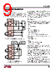
9 / 20 page  9 LTC1693 Driver Electrical Isolation The LTC1693-1 and LTC1693-2 incorporate two individual drivers in a single package that can be separately connected to GND and VCC connections. Figure 2 shows a circuit with an LTC1693-2, its top driver left floating while the bottom driver is powered with respect to ground. Similarly Figure 3 shows a simplified circuit of a LTC1693-1 which is driv- ing MOSFETs with different ground potentials. Because there is 1G Ω of isolation between these drivers in a single package, ground current on the secondary side will not recirculate to the primary side of the circuit. Power Dissipation To ensure proper operation and long term reliability, the LTC1693 must not operate beyond its maximum tempera- ture rating. Package junction temperature can be calcu- lated by: TJ = TA + PD(θJA) where: TJ = Junction Temperature TA = Ambient Temperature PD = Power Dissipation θJA = Junction-to-Ambient Thermal Resistance Power dissipation consists of standby and switching power losses: PD = PSTDBY + PAC where: PSTDBY = Standby Power Losses PAC = AC Switching Losses The LTC1693 consumes very little current during standby. This DC power loss per driver at VCC = 12V is only (360 µA)(12V) = 4.32mW. AC switching losses are made up of the output capacitive load losses and the transition state losses. The capactive load losses are primarily due to the large AC currents needed to charge and discharge the load capacitance during switching. Load losses for the CMOS driver driving a pure capacitive load COUT will be: Load Capacitive Power (COUT) = (COUT)(f)(VCC)2 The power MOSFET’s gate capacitance seen by the driver output varies with its VGS voltage level during switching. A power MOSFET’s capacitive load power dissipation can be calculated by its gate charge factor, QG. The QG value Figure 2. Simplified LTC1693-2 Floating Driver Application Figure 3. Simplified LTC1693-1 Application with Different Ground Potentials OUT1 IN1 GND1 VCC1 VCC2 V + •• V + LTC1693-1 OTHER PRIMARY-SIDE CIRCUITS OTHER SECONDARY-SIDE CIRCUITS OUT2 IN2 GND2 1693 F03 APPLICATIONS INFORMATION OUT1 IN1 GND1 VCC1 VCC2 V + VIN LTC1693-2 N1 OUT2 IN2 GND2 N2 1693 F02 • |
|
|
ссылки URL |
| Вашему бизинису помогли Аллдатащит? [ DONATE ] |
Что такое Аллдатащит | реклама | контакт | Конфиденциальность | Ссылка на техническое описание | обмен ссыками | поиск по производителю All Rights Reserved©Alldatasheet.com |
| Russian : Alldatasheetru.com | Korean : Alldatasheet.co.kr | Spanish : Alldatasheet.es | French : Alldatasheet.fr | Italian : Alldatasheetit.com Portuguese : Alldatasheetpt.com | Polish : Alldatasheet.pl | Vietnamese : Alldatasheet.vn Indian : Alldatasheet.in | Mexican : Alldatasheet.com.mx | British : Alldatasheet.co.uk | New Zealand : Alldatasheet.co.nz |
|
Family Site : ic2ic.com |
icmetro.com |
 Russian ▼
 English
 Chinese
 German
 Japanese
 Russian
 Korean
 Spanish
 French
 Italian
 Portuguese
 Polish
 Vietnamese
 Indian
 Mexican
 British
 New Zealand