|
поискавой системы для электроныых деталей |
|
|
поискавой системы для электроныых деталей |
|
ADP1046ACPZ-R7 датащи(PDF) 89 Page - Analog Devices |
|
|
|||||||||||||||||||||||||||||
ADP1046ACPZ-R7 датащи(HTML) 89 Page - Analog Devices |
|
|
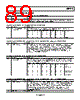
89 / 96 page  Data Sheet ADP1046 Rev. 0 | Page 89 of 96 RESONANT MODE REGISTER DESCRIPTIONS Table 153. Register 0x40—PWM Switching Frequency Setting in Resonant Mode Bits Bit Name R/W Description [7:6] Reserved R/W Reserved. [5:0] Switching frequency R/W This register sets the switching frequency of the PWM pins and enables resonant mode. To enable resonant mode, set these bits to 0x3F (111111). Table 154. Register 0x41—OUTA Rising Edge Dead Time in Resonant Mode Bits Bit Name R/W Description [7:0] Δt1 (rising edge dead time of OUTA) R/W This register sets Δt1, which is the delay of the rising edge of OUTA from the start of the switching cycle, tA. Each LSB corresponds to 5 ns of resolution. Bit 7 Bit 6 Bit 5 Bit 4 Bit 3 Bit 2 Bit 1 Bit 0 Δt1 (ns) 0 0 0 0 0 0 0 0 0 0 0 0 0 0 0 0 1 5 … … … … … … … … … 1 1 1 1 1 1 1 1 1275 Table 155. Register 0x42—Lowest Switching Frequency Limit Setting (Maximum Switching Cycle in Resonant Mode) Bits Bit Name R/W Description [7:0] Lowest frequency R/W This register contains the eight MSBs of the 12-bit value of the lowest switching frequency (maxi- mum switching cycle) limit. This value is always used with the top four bits of Register 0x44, which contain the four LSBs of the lowest switching frequency limit. Each LSB of the 12-bit value corresponds to 5 ns of resolution for the switching cycle. For example, if Register 0x42 is set to 0xA0 (160 decimal) and Bits[7:4] of Register 0x44 are set to 0xF (15 decimal), the maximum switching cycle is (160 × 16 + 15) × 5 ns = 12.875 μs, and the lowest switching frequency limit is 1/12.875 μs = 77.7 kHz. Table 156. Register 0x43—OUTA Falling Edge Dead Time in Resonant Mode Bits Bit Name R/W Description [7:0] Δt2 (falling edge dead time of OUTA) R/W This register sets Δt2, which is the difference between the falling edge of OUTA and the mid- point of the switching cycle, tB. Each LSB corresponds to 5 ns of resolution. When the register value is from 0x00 to 0x7F, the falling edge of OUTA is trailing tB. When the value is from 0x80 to 0xFF, the falling edge of OUTA is leading tB. Bit 7 Bit 6 Bit 5 Bit 4 Bit 3 Bit 2 Bit 1 Bit 0 Δt2 0 0 0 0 0 0 0 0 0 ns 0 0 0 0 0 0 0 1 5 ns trailing … … … … … … … … … 0 1 1 1 1 1 1 1 635 ns trailing 1 0 0 0 0 0 0 0 640 ns leading … … … … … … … … … 1 1 1 1 1 1 1 1 5 ns leading Table 157. Register 0x44—Lowest Switching Frequency Limit Setting (Maximum Switching Cycle in Resonant Mode) Bits Bit Name R/W Description [7:4] Lowest frequency R/W This register contains the four LSBs of the 12-bit value of the lowest switching frequency (maxi- mum switching cycle) limit. This value is always used with the eight bits of Register 0x42, which contain the eight MSBs of the lowest switching frequency limit. Each LSB of the 12-bit value corresponds to 5 ns of resolution for the switching cycle. For example, if Register 0x42 is set to 0xA0 (160 decimal) and Bits[7:4] of Register 0x44 are set to 0xF (15 decimal), the maximum switching cycle is (160 × 16 + 15) × 5 ns = 12.875 μs, and the lowest switching frequency limit is 1/12.875 μs = 77.7 kHz. [3:0] Reserved R/W Reserved. |
|
ссылки URL |
| Вашему бизинису помогли Аллдатащит? [ DONATE ] |
Что такое Аллдатащит | реклама | контакт | Конфиденциальность | Ссылка на техническое описание | обмен ссыками | поиск по производителю All Rights Reserved©Alldatasheet.com |
| Russian : Alldatasheetru.com | Korean : Alldatasheet.co.kr | Spanish : Alldatasheet.es | French : Alldatasheet.fr | Italian : Alldatasheetit.com Portuguese : Alldatasheetpt.com | Polish : Alldatasheet.pl | Vietnamese : Alldatasheet.vn Indian : Alldatasheet.in | Mexican : Alldatasheet.com.mx | British : Alldatasheet.co.uk | New Zealand : Alldatasheet.co.nz |
|
Family Site : ic2ic.com |
icmetro.com |
 Russian ▼
 English
 Chinese
 German
 Japanese
 Russian
 Korean
 Spanish
 French
 Italian
 Portuguese
 Polish
 Vietnamese
 Indian
 Mexican
 British
 New Zealand