|
поискавой системы для электроныых деталей |
|
|
поискавой системы для электроныых деталей |
|
WM5628L датащи(PDF) 11 Page - Wolfson Microelectronics plc |
|
|
|||||||||||||||||||||||||||||
WM5628L датащи(HTML) 11 Page - Wolfson Microelectronics plc |
|
|
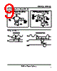
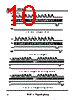
11 / 15 page  WM5628L, WM5628 Wolfson Microelectronics 11 Pin Descriptions Pin Name Type Function 1 DACB Analogue output DAC B output 2 DACA Analogue input DAC A output 3 GND Supply Ground return 4 Data Digital input Serial data input 5 CLK Digital input Serial interface clock, negative edge sensitive 6VDD Supply Positive supply voltage 7 DACE Analogue output DAC E output 8 DACF Analogue output DAC F output 9 DACG Analogue output DAC G output 10 DACH Analogue output DAC H output 11 Ref2 Analogue input Reference to DACE, DACF, DACG and DACH 12 Load Digital input Serial input load 13 LDAC Digital input DAC update latch control 14 Ref1 Analogue input Reference to DACA, DACB, DACC and DACD 15 DACD Analogue output DAC D output 16 DACC Analogue output DAC C output Functional Description DAC operation Each of WM5628/L 's eight digital to analogue converters (DACs) are implemented using a single resistor string with 256 taps corresponding to each of the input 8-bit codes. One end of a resistor string is connected to the GND pin and the other end is driven from the output of a reference input buffer. The use of a resistor string guarantees monotonicity of the DAC's output voltage. Linearity depends upon the matching of the resistor string's individual elements and the performance of the output buffer. Two high input impedance voltage reference buffers are provided, each driving four DACs, Each DAC has a voltage output amplifier which is programmable for gains of x1 or x 2 through the serial interface. The DAC output amplifiers feature rail to rail output stages, allowing outputs over the full supply voltage range to be achieved with a x 2 gain setting and a VDD/2 reference voltage input. Used in this way a slight degradation in linearity will occur as the output voltage approaches VDD. A power-on-reset activates at power up resetting the DACs inputs to code 0. Each output voltage is given by: Vout = Vref x CODE/256 x (RNG+1 ) Where: RNG controls the output gains of x 1 and x 2 CODE is the range 0 to 255 Data Interface WM5628/L's eight double buffered DAC inputs allow several ways of controlling the update of each DAC's output. Serial data is input, MSB first, into the DATA input pin Serial Input DAC Address and Output Tables using CLK, LOAD and LDAC control inputs and comprises 3 DAC address bits, an output range (RNG) bit and 8 DAC input bits. With the LOAD pin high data is clocked into the DATA pin on each falling edge of CLK. Any number of data bits may be clocked in, only the last 12 bits are used. When all data bits have been clocked in, a falling edge at the LOAD pin latches the data and RNG bits into the correct 9 bit input latch using the 3 bit DAC address. If the LDAC input pin is low, the second latch at the DAC input is transparent, and the DAC input and RNG bit will be updated on the falling edge of LOAD simultaneously with the input latch, as shown in figure 1. If the LDAC input is high during serial data input, as shown in figure 2, the falling edge of the LOAD input stores the data in the addressed input latch. The falling edge of LDAC updates the second latches from the input latches and hence the DAC outputs. |
|
|
ссылки URL |
| Вашему бизинису помогли Аллдатащит? [ DONATE ] |
Что такое Аллдатащит | реклама | контакт | Конфиденциальность | Ссылка на техническое описание | обмен ссыками | поиск по производителю All Rights Reserved©Alldatasheet.com |
| Russian : Alldatasheetru.com | Korean : Alldatasheet.co.kr | Spanish : Alldatasheet.es | French : Alldatasheet.fr | Italian : Alldatasheetit.com Portuguese : Alldatasheetpt.com | Polish : Alldatasheet.pl | Vietnamese : Alldatasheet.vn Indian : Alldatasheet.in | Mexican : Alldatasheet.com.mx | British : Alldatasheet.co.uk | New Zealand : Alldatasheet.co.nz |
|
Family Site : ic2ic.com |
icmetro.com |
 Russian ▼
 English
 Chinese
 German
 Japanese
 Russian
 Korean
 Spanish
 French
 Italian
 Portuguese
 Polish
 Vietnamese
 Indian
 Mexican
 British
 New Zealand