|
поискавой системы для электроныых деталей |
|
|
поискавой системы для электроныых деталей |
|
ICS1893CF датащи(PDF) 103 Page - Integrated Device Technology |
|
|
|||||||||||||||||||||||||||||
ICS1893CF датащи(HTML) 103 Page - Integrated Device Technology |
|
|
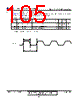
103 / 127 page  Chapter 9 DC and AC Operating Conditions ICS1893CF, Rev. J, 08/11/09 August, 2009 103 ICS1893CF Data Sheet Rev. J - Release Copyright © 2009, Integrated Device Technology, Inc. All rights reserved. 9.5 Timing Diagrams 9.5.1 Timing for Clock Reference In (REF_IN) Pin Table 9-8 lists the significant time periods for signals on the clock reference in (REF_IN) pin. Figure 9-2 shows the timing diagram for the time periods. Note: The REF_IN switching point is 50% of VDD. Figure 9-2. REF_IN Timing Diagram Table 9-8. REF_IN Timing Time Period Parameter Conditions Min. Typ. Max. Units t1 REF_IN Duty Cycle – 45 50 55 % t2 REF_IN Period – – 40 – ns REF_IN t1 t2 |
|
ссылки URL |
| Вашему бизинису помогли Аллдатащит? [ DONATE ] |
Что такое Аллдатащит | реклама | контакт | Конфиденциальность | Ссылка на техническое описание | обмен ссыками | поиск по производителю All Rights Reserved©Alldatasheet.com |
| Russian : Alldatasheetru.com | Korean : Alldatasheet.co.kr | Spanish : Alldatasheet.es | French : Alldatasheet.fr | Italian : Alldatasheetit.com Portuguese : Alldatasheetpt.com | Polish : Alldatasheet.pl | Vietnamese : Alldatasheet.vn Indian : Alldatasheet.in | Mexican : Alldatasheet.com.mx | British : Alldatasheet.co.uk | New Zealand : Alldatasheet.co.nz |
|
Family Site : ic2ic.com |
icmetro.com |
 Russian ▼
 English
 Chinese
 German
 Japanese
 Russian
 Korean
 Spanish
 French
 Italian
 Portuguese
 Polish
 Vietnamese
 Indian
 Mexican
 British
 New Zealand