|
поискавой системы для электроныых деталей |
|
|
поискавой системы для электроныых деталей |
|
MAX5500AGAP+ датащи(PDF) 12 Page - Maxim Integrated Products |
|
|
|||||||||||||||||||||||||||||
MAX5500AGAP+ датащи(HTML) 12 Page - Maxim Integrated Products |
|
|
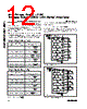
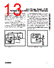
12 / 14 page  Low-Power, Quad, 12-Bit Voltage-Output DACs with Serial Interface 12 ______________________________________________________________________________________ DAC CONTENTS ANALOG OUTPUT MSB LSB 4095 1111 1111 1111 +VREF ( ——— ) 4096 2049 1000 0000 0001 +VREF ( ——— ) 4096 2048 +VREF 1000 0000 0000 +VREF ( ——— ) = ———— 4096 2 2047 0111 1111 1111 +VREF ( ——— ) 4096 1 0000 0000 0001 +VREF ( ——— ) 4096 0000 0000 0000 0V Table 2. Unipolar Code Table DAC CONTENTS ANALOG OUTPUT MSB LSB 2047 1111 1111 1111 +VREF ( ——— ) 2048 1 1000 0000 0001 +VREF ( ——— ) 2048 1000 0000 0000 0V 1 0111 1111 1111 -VREF ( ——— ) 2048 2047 0000 0000 0001 -VREF ( ——— ) 2048 2048 0000 0000 0000 -VREF ( ——— ) = -VREF 2048 Table 3. Bipolar Code Table Note: 1 LSB = (VREF) ( 4096 ) 1 MAX5500 MAX5501 DAC A DAC B DAC C DAC D OUTA FBA FBB FBC FBD OUTB OUTC OUTD DGND AGND REFAB REFCD REFERENCE INPUTS +5V VDD Figure 9. Unipolar Output Circuit MAX5500 MAX5501 DAC A DAC B DAC C DAC D VREFAB = VREFCD = 2.5V OUTA 10kΩ 10kΩ 10kΩ 10kΩ 10kΩ 10kΩ 10kΩ 10kΩ OUTB OUTC OUTD DGND AGND REFAB REFCD REFERENCE INPUTS +5V VDD FBA FBB FBC FBD Figure 10. Unipolar Rail-to-Rail Output Circuit Applications Information Unipolar Output For a unipolar output, the output voltages and the refer- ence inputs are of the same polarity. Figure 9 shows the MAX5500/MAX5501 unipolar output circuit, which is also the typical operating circuit. Table 2 lists the unipo- lar output codes. See Figure 10 for rail-to-rail outputs. Figure 10 shows the MAX5500/MAX5501 with the output amplifiers con- figured with a closed-loop gain of +2 to provide 0 to 5V full-scale range with a 2.5V external reference voltage. Bipolar Output Figure 11 shows the MAX5500/MAX5501 configured for bipolar operation. VOUT = VREF [(2NB/4096) - 1] where NB is the numeric value of the DAC’s binary input code. Table 3 shows digital codes (offset binary) and corresponding output voltages for the circuit of Figure 11. |
|
|
ссылки URL |
| Вашему бизинису помогли Аллдатащит? [ DONATE ] |
Что такое Аллдатащит | реклама | контакт | Конфиденциальность | Ссылка на техническое описание | обмен ссыками | поиск по производителю All Rights Reserved©Alldatasheet.com |
| Russian : Alldatasheetru.com | Korean : Alldatasheet.co.kr | Spanish : Alldatasheet.es | French : Alldatasheet.fr | Italian : Alldatasheetit.com Portuguese : Alldatasheetpt.com | Polish : Alldatasheet.pl | Vietnamese : Alldatasheet.vn Indian : Alldatasheet.in | Mexican : Alldatasheet.com.mx | British : Alldatasheet.co.uk | New Zealand : Alldatasheet.co.nz |
|
Family Site : ic2ic.com |
icmetro.com |
 Russian ▼
 English
 Chinese
 German
 Japanese
 Russian
 Korean
 Spanish
 French
 Italian
 Portuguese
 Polish
 Vietnamese
 Indian
 Mexican
 British
 New Zealand