|
поискавой системы для электроныых деталей |
|
|
поискавой системы для электроныых деталей |
|
MAX5500AGAP+ датащи(PDF) 8 Page - Maxim Integrated Products |
|
|
|||||||||||||||||||||||||||||
MAX5500AGAP+ датащи(HTML) 8 Page - Maxim Integrated Products |
|
|
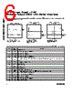
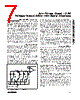
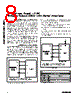
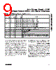
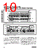
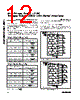
8 / 14 page  Low-Power, Quad, 12-Bit Voltage-Output DACs with Serial Interface 8 _______________________________________________________________________________________ SCLK DIN DOUT* CS SK SO SI* I/O MAX5500 MAX5501 MICROWIRE PORT *THE DOUT-SI CONNECTION IS NOT REQUIRED FOR WRITING TO THE MAX5500/MAX5501, BUT CAN BE USED FOR READBACK PURPOSES. Figure 2. Connections for MICROWIRE Serial-Interface Configurations The MAX5500/MAX5501s’ 3-wire serial interface is compatible with both MICROWIRE (Figure 2) and SPI/QSPI (Figure 3). The serial input word consists of two address bits and two control bits followed by 12 data bits (MSB first), as shown in Figure 4. The 4-bit address/control code determines the MAX5500/ MAX5501s’ response outlined in Table 1. The connec- tion between DOUT and the serial-interface port is not necessary, but may be used for data echo. Data held in the shift register can be shifted out of DOUT and returned to the µP for data verification. The digital inputs of the MAX5500/MAX5501 are double buffered. Depending on the command issued through the serial interface, the input register(s) can be loaded without affecting the DAC register(s), the DAC register(s) can be loaded directly, or all four DAC registers can be updated simultaneously from the input registers (Table 1). Serial-Interface Description The MAX5500/MAX5501 require 16 bits of serial data. Table 1 lists the serial-interface programming com- mands. For certain commands, the 12 data bits are don’t-care bits. Data is sent MSB first and can be sent in two 8-bit packets or one 16-bit word ( CS must remain low until 16 bits are transferred). The serial data is com- posed of two DAC address bits (A1, A0) and two control bits (C1, C0), followed by the 12 data bits D11–D0 (Figure 4). The 4-bit address/control code determines: • The register(s) to be updated • The clock edge on which data is to be clocked out through the serial-data output (DOUT) • The state of the user-programmable logic output (UPO) • If the device is to enter shutdown mode (assuming PDL is high) • How the device is configured when exiting out of shutdown mode DOUT* DIN SCLK CS MISO* MOSI SCK I/O SPI/QSPI PORT SS +5V CPOL = 0, CPHA = 0 *THE DOUT-MISO CONNECTION IS NOT REQUIRED FOR WRITING TO THE MAX5500/MAX5501, BUT CAN BE USED FOR READBACK PURPOSES. MAX5500 MAX5501 Figure 3. Connections for SPI/QSPI MSB.................................................................................................................................LSB MSB...........................................................................................LSB 16 BITS OF SERIAL DATA ADDRESS BITS CONTROL BITS DATA BITS 4 ADDRESS/ CONTROL BITS D11..............................................................................................D0 A1 A0 C1 C0 12 DATA BITS Figure 4. Serial-Data Format |
|
|
ссылки URL |
| Вашему бизинису помогли Аллдатащит? [ DONATE ] |
Что такое Аллдатащит | реклама | контакт | Конфиденциальность | Ссылка на техническое описание | обмен ссыками | поиск по производителю All Rights Reserved©Alldatasheet.com |
| Russian : Alldatasheetru.com | Korean : Alldatasheet.co.kr | Spanish : Alldatasheet.es | French : Alldatasheet.fr | Italian : Alldatasheetit.com Portuguese : Alldatasheetpt.com | Polish : Alldatasheet.pl | Vietnamese : Alldatasheet.vn Indian : Alldatasheet.in | Mexican : Alldatasheet.com.mx | British : Alldatasheet.co.uk | New Zealand : Alldatasheet.co.nz |
|
Family Site : ic2ic.com |
icmetro.com |
 Russian ▼
 English
 Chinese
 German
 Japanese
 Russian
 Korean
 Spanish
 French
 Italian
 Portuguese
 Polish
 Vietnamese
 Indian
 Mexican
 British
 New Zealand