|
поискавой системы для электроныых деталей |
|
|
поискавой системы для электроныых деталей |
|
ST7FOXK2 датащи(PDF) 192 Page - STMicroelectronics |
|
|
|||||||||||||||||||||||||||||
ST7FOXK2 датащи(HTML) 192 Page - STMicroelectronics |
|
|
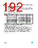
192 / 226 page  Electrical characteristics ST7FOXF1, ST7FOXK1, ST7FOXK2 192/226 12.4 Supply current characteristics The following current consumption specified for the ST7 functional operating modes over temperature range does not take into account the clock source current consumption. To get the total device consumption, the two current values must be added (except for Halt mode for which the clock is stopped). 12.4.1 Supply current TA = -40 to +85 °C unless otherwise specified. Table 72. Supply current characteristics Symbol Parameter Conditions Typ Max Unit IDD Supply current in Run mode(1) fCPU = 4 MHz 2.5 4.5(2) mA fCPU = 8 MHz 5.0 9 Supply current in Wait mode(3) fCPU = 4 MHz 1.1 2(2) fCPU = 8 MHz 2 3.5 Supply current in Slow mode(4) fCPU/32 = 250 kHz 550 950 µA Supply current in Slow-Wait mode(5) fCPU/32 = 250 kHz 450 750 Supply current in AWUFH mode(6)(7) 50 100(2) Supply current in Active Halt mode 120 250 Supply current in Halt mode(8) TA = 85 °C 0.5 5 1. CPU running with memory access, all I/O pins in input mode with a static value at VDD or VSS (no load), all peripherals in reset state; clock input (CLKIN) driven by external square wave, LVD disabled. 2. Data based on characterization, not tested in production. 3. All I/O pins in input mode with a static value at VDD or VSS (no load), all peripherals in reset state; clock input (CLKIN) driven by external square wave, LVD disabled. 4. Slow mode selected with fCPU based on fOSC divided by 32. All I/O pins in input mode with a static value at VDD or VSS (no load), all peripherals in reset state; clock input (CLKIN) driven by external square wave, LVD disabled. 5. Slow-Wait mode selected with fCPU based on fOSC divided by 32. All I/O pins in input mode with a static value at VDD or VSS (no load), all peripherals in reset state; clock input (CLKIN) driven by external square wave, LVD disabled. 6. All I/O pins in input mode with a static value at VDD or VSS (no load). Data tested in production at VDD max. and fCPU max. 7. This consumption refers to the Halt period only and not the associated run period which is software dependent. 8. All I/O pins in output mode with a static value at VSS (no load), LVD disabled. Data based on characterization results, tested in production at VDD max and fCPU max. |
|
ссылки URL |
| Вашему бизинису помогли Аллдатащит? [ DONATE ] |
Что такое Аллдатащит | реклама | контакт | Конфиденциальность | Ссылка на техническое описание | обмен ссыками | поиск по производителю All Rights Reserved©Alldatasheet.com |
| Russian : Alldatasheetru.com | Korean : Alldatasheet.co.kr | Spanish : Alldatasheet.es | French : Alldatasheet.fr | Italian : Alldatasheetit.com Portuguese : Alldatasheetpt.com | Polish : Alldatasheet.pl | Vietnamese : Alldatasheet.vn Indian : Alldatasheet.in | Mexican : Alldatasheet.com.mx | British : Alldatasheet.co.uk | New Zealand : Alldatasheet.co.nz |
|
Family Site : ic2ic.com |
icmetro.com |
 Russian ▼
 English
 Chinese
 German
 Japanese
 Russian
 Korean
 Spanish
 French
 Italian
 Portuguese
 Polish
 Vietnamese
 Indian
 Mexican
 British
 New Zealand