|
поискавой системы для электроныых деталей |
|
|
поискавой системы для электроныых деталей |
|
ST7FOXK2 датащи(PDF) 188 Page - STMicroelectronics |
|
|
|||||||||||||||||||||||||||||
ST7FOXK2 датащи(HTML) 188 Page - STMicroelectronics |
|
|
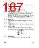
188 / 226 page  Electrical characteristics ST7FOXF1, ST7FOXK1, ST7FOXK2 188/226 Figure 82. Pin input voltage 12.2 Absolute maximum ratings Stresses above those listed as “absolute maximum ratings” may cause permanent damage to the device. This is a stress rating only and functional operation of the device under these conditions is not implied. Exposure to maximum rating conditions for extended periods may affect device reliability. VIN ST7 PIN Table 66. Voltage characteristics Symbol Ratings Maximum value Unit VDD - VSS Supply voltage 7.0 V VIN Input voltage on any pin(1)(2) 1. Directly connecting the RESET and I/O pins to VDD or VSS could damage the device if an unintentional internal reset is generated or an unexpected change of the I/O configuration occurs (for example, due to a corrupted Program Counter). To guarantee safe operation, this connection has to be done through a pull- up or pull-down resistor (typical: 4.7 k Ω for RESET, 10 kΩ for I/Os). Unused I/O pins must be tied in the same way to VDD or VSS according to their reset configuration. 2. IINJ(PIN) must never be exceeded. This is implicitly insured if VIN maximum is respected. If VIN maximum cannot be respected, the injection current must be limited externally to the IINJ(PIN) value. A positive injection is induced by VIN>VDD while a negative injection is induced by VIN<VSS. For true open-drain pads, there is no positive injection current, and the corresponding VIN maximum must always be respected VSS-0.3 to VDD+0.3 VESD(HBM) Electrostatic discharge voltage (Human Body model) see Section 12.8.3 on page 203 VESD(CDM) Electrostatic discharge voltage (Charge Device model) |
|
ссылки URL |
| Вашему бизинису помогли Аллдатащит? [ DONATE ] |
Что такое Аллдатащит | реклама | контакт | Конфиденциальность | Ссылка на техническое описание | обмен ссыками | поиск по производителю All Rights Reserved©Alldatasheet.com |
| Russian : Alldatasheetru.com | Korean : Alldatasheet.co.kr | Spanish : Alldatasheet.es | French : Alldatasheet.fr | Italian : Alldatasheetit.com Portuguese : Alldatasheetpt.com | Polish : Alldatasheet.pl | Vietnamese : Alldatasheet.vn Indian : Alldatasheet.in | Mexican : Alldatasheet.com.mx | British : Alldatasheet.co.uk | New Zealand : Alldatasheet.co.nz |
|
Family Site : ic2ic.com |
icmetro.com |
 Russian ▼
 English
 Chinese
 German
 Japanese
 Russian
 Korean
 Spanish
 French
 Italian
 Portuguese
 Polish
 Vietnamese
 Indian
 Mexican
 British
 New Zealand