|
поискавой системы для электроныых деталей |
|
|
поискавой системы для электроныых деталей |
|
ADL5906ACPZN-R2 датащи(PDF) 9 Page - Analog Devices |
|
|
|||||||||||||||||||||||||||||
ADL5906ACPZN-R2 датащи(HTML) 9 Page - Analog Devices |
|
|
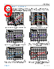
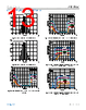
9 / 30 page  Data Sheet ADL5906 TYPICAL PERFORMANCE CHARACTERISTICS analog.com Rev. B | 9 of 30 VPOS1 = VPOS2 = 5 V, single-ended input drive, VRMS connected to VSET, VTGT = 0.8 V, CRMS = 0.1 µF, TA = +25°C (green), −55°C (light blue), −40°C (blue), +85°C (red), +105°C (orange), and +125°C (black), where appropriate. Error referred to slope and intercept at indicated calibration points. Input RF signal is a sine wave (CW), unless otherwise indicated. Figure 3. Typical VRMS vs. Input Power (dBm) vs. Frequency (10 MHz to 10 GHz) at 25°C Figure 4. Error from CW Linear Reference vs. Signal Modulation (QPSK, 16 QAM, 64 QAM), Frequency = 900 MHz Figure 5. Error from CW Linear Reference vs. Signal Modulation (CDMA 2000, One-Carrier W-CDMA, Four-Carrier W-CDMA), Frequency = 2.14 GHz Figure 6. Typical VRMS vs. Frequency for Six RF Input Levels Figure 7. Error from CW Linear Reference vs. Signal Modulation (QPSK, 16 QAM, 64 QAM), Frequency = 2.14 GHz, Three Point Calibration at 0 dBm, −40 dBm, and −55 dBm Figure 8. Error from CW Linear Reference vs. Signal Modulation (LTE TM1 One-Carrier, 20 MHz), Frequency = 2.14 GHz, Three Point Calibration at 0 dBm, −40 dBm, and −55 dBm |
|
ссылки URL |
| Вашему бизинису помогли Аллдатащит? [ DONATE ] |
Что такое Аллдатащит | реклама | контакт | Конфиденциальность | Ссылка на техническое описание | обмен ссыками | поиск по производителю All Rights Reserved©Alldatasheet.com |
| Russian : Alldatasheetru.com | Korean : Alldatasheet.co.kr | Spanish : Alldatasheet.es | French : Alldatasheet.fr | Italian : Alldatasheetit.com Portuguese : Alldatasheetpt.com | Polish : Alldatasheet.pl | Vietnamese : Alldatasheet.vn Indian : Alldatasheet.in | Mexican : Alldatasheet.com.mx | British : Alldatasheet.co.uk | New Zealand : Alldatasheet.co.nz |
|
Family Site : ic2ic.com |
icmetro.com |
 Russian ▼
 English
 Chinese
 German
 Japanese
 Russian
 Korean
 Spanish
 French
 Italian
 Portuguese
 Polish
 Vietnamese
 Indian
 Mexican
 British
 New Zealand