|
поискавой системы для электроныых деталей |
|
|
поискавой системы для электроныых деталей |
|
PIC16F631 датащи(PDF) 111 Page - Microchip Technology |
|
|
|||||||||||||||||||||||||||||
PIC16F631 датащи(HTML) 111 Page - Microchip Technology |
|
|
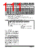
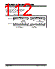
111 / 294 page  © 2007 Microchip Technology Inc. DS41262D-page 109 PIC16F631/677/685/687/689/690 TABLE 9-1: ADC CLOCK PERIOD (TAD) VS. DEVICE OPERATING FREQUENCIES (VDD > 3.0V) FIGURE 9-2: ANALOG-TO-DIGITAL CONVERSION TAD CYCLES 9.1.5 INTERRUPTS The ADC module allows for the ability to generate an interrupt upon completion of an Analog-to-Digital conversion. The ADC interrupt flag is the ADIF bit in the PIR1 register. The ADC interrupt enable is the ADIE bit in the PIE1 register. The ADIF bit must be cleared in software. This interrupt can be generated while the device is operating or while in Sleep. If the device is in Sleep, the interrupt will wake-up the device. Upon waking from Sleep, the next instruction following the SLEEP instruction is always executed. If the user is attempting to wake-up from Sleep and resume in-line code execution, the global interrupt must be disabled. If the global interrupt is enabled, execution will switch to the interrupt service routine. Please see Section 9.1.5 “Interrupts” for more information. ADC Clock Period (TAD) Device Frequency (FOSC) ADC Clock Source ADCS<2:0> 20 MHz 8 MHz 4 MHz 1 MHz FOSC/2 000 100 ns(2) 250 ns(2) 500 ns(2) 2.0 μs FOSC/4 100 200 ns(2) 500 ns(2) 1.0 μs(2) 4.0 μs FOSC/8 001 400 ns(2) 1.0 μs(2) 2.0 μs 8.0 μs(3) FOSC/16 101 800 ns(2) 2.0 μs4.0 μs 16.0 μs(3) FOSC/32 010 1.6 μs4.0 μs 8.0 μs(3) 32.0 μs(3) FOSC/64 110 3.2 μs 8.0 μs(3) 16.0 μs(3) 64.0 μs(3) FRC x11 2-6 μs(1,4) 2-6 μs(1,4) 2-6 μs(1,4) 2-6 μs(1,4) Legend: Shaded cells are outside of recommended range. Note 1: The FRC source has a typical TAD time of 4 μs for VDD > 3.0V. 2: These values violate the minimum required TAD time. 3: For faster conversion times, the selection of another clock source is recommended. 4: When the device frequency is greater than 1 MHz, the FRC clock source is only recommended if the conversion will be performed during Sleep. TAD1 TAD2 TAD3 TAD4 TAD5 TAD6 TAD7 TAD8 TAD9 Set GO/DONE bit Holding Capacitor is disconnected from analog input (typically 100 ns) b9 b8 b7 b6 b5 b4 b3 b2 TAD10 TAD11 b1 b0 TCY to TAD Conversion Starts ADRESH and ADRESL registers are loaded, GO bit is cleared, ADIF bit is set, Holding capacitor is connected to analog input Note: The ADIF bit is set at the completion of every conversion, regardless of whether or not the ADC interrupt is enabled. |
|
ссылки URL |
| Вашему бизинису помогли Аллдатащит? [ DONATE ] |
Что такое Аллдатащит | реклама | контакт | Конфиденциальность | Ссылка на техническое описание | обмен ссыками | поиск по производителю All Rights Reserved©Alldatasheet.com |
| Russian : Alldatasheetru.com | Korean : Alldatasheet.co.kr | Spanish : Alldatasheet.es | French : Alldatasheet.fr | Italian : Alldatasheetit.com Portuguese : Alldatasheetpt.com | Polish : Alldatasheet.pl | Vietnamese : Alldatasheet.vn Indian : Alldatasheet.in | Mexican : Alldatasheet.com.mx | British : Alldatasheet.co.uk | New Zealand : Alldatasheet.co.nz |
|
Family Site : ic2ic.com |
icmetro.com |
 Russian ▼
 English
 Chinese
 German
 Japanese
 Russian
 Korean
 Spanish
 French
 Italian
 Portuguese
 Polish
 Vietnamese
 Indian
 Mexican
 British
 New Zealand