|
поискавой системы для электроныых деталей |
|
|
поискавой системы для электроныых деталей |
|
34717 датащи(PDF) 14 Page - Freescale Semiconductor, Inc |
|
|
|||||||||||||||||||||||||||||
34717 датащи(HTML) 14 Page - Freescale Semiconductor, Inc |
|
|
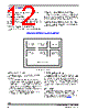
14 / 25 page  Analog Integrated Circuit Device Data 14 Freescale Semiconductor 34717 FUNCTIONAL DEVICE OPERATION OPERATIONAL MODES FUNCTIONAL DEVICE OPERATION OPERATIONAL MODES Figure 5. Operation Modes Diagram MODES OF OPERATION The 34717 has two primary modes of operation: Normal Mode In Normal Mode, all functions and outputs are fully operational. To be in this mode, the VIN needs to be within its operating range, Shutdown input is high, and no faults are present. This mode consumes the most amount of power. Shutdown Mode In this mode, activated by pulling the SD pin low, the chip is in a shutdown state and the output is disabled and discharged. In this mode, the 34717 consumes the least amount of power since almost all of the internal blocks are disabled. START-UP SEQUENCE When power is first applied, the 34717 checks the status of the SD pin. If the device is in a shutdown mode, no block will power up and the output will not attempt to ramp. Once the SD pin is set to high, the VDDI internal supply voltage and the bias currents will be established, so the internal VDDI POR signal can be released. The rest of the internal blocks will be enabled and the buck converter switching frequency and soft start timing values are determined by reading the FREQ, ILIM1, and ILIM2 pins. A soft start cycle is then initiated to ramp up the output of the buck converter. The first channel uses an internal 0.7 V reference for its error amplifier while the second channel’s error amplifier uses the voltage on the VREFIN pin as its reference voltage until VREFIN is equal to 0.7 V, then the error amplifier defaults to the internal 0.7 V reference voltage. This method allows the second output to achieve multiple tracking configurations as will be explained later in this document. Soft start is used to prevent the output voltage from overshooting during startup. At initial startup, the output capacitor is at zero volts; VOUT = 0 V. Therefore, the voltage across the inductor will be PVIN during the capacitor charge phase which will create a very sharp di/dt ramp. Allowing the inductor current to rise too high can result in a large difference between the charging current and the actual load T J > = 170˚C Shutdown V OUT1 = Discharge V OUT2 = Discharge PG = 1 SD = 0 SD = 1 3.0V < = V IN < = 6.0V Power Off V OUT1 = OFF V OUT2 = OFF PG = 1 V IN < 3.0V Normal Fsw is programmed I LIM1, ILIM2 are programmed V OUT1 and VOUT2 tSS = 1 V OUT1 = ON V OUT2 = ON PG = 0 V OUT1 Short Circuit V OUT1 = OFF V OUT2 = ON PG = 1 t TIMEOUT = 1 Channel 1 Overcurrent V OUT1 = OFF V OUT2 = ON PG = 1 t TIMEOUT = 1 Channel 1 Thermal Shutdown V OUT1 = OFF V OUT2 = ON PG = 1 V OUT1 Overvoltage V OUT1 = ON V OUT2 = ON PG = 1 V OUT1 Undervoltage V OUT1 = ON V OUT2 = ON PG = 1 V OUT2 Short Circuit V OUT1 = ON V OUT2 = OFF PG = 1 t TIMEOUT = 1 Channel 2 Overcurrent V OUT1 = ON V OUT2 = OFF PG = 1 t TIMEOUT = 1 Channel 2 Thermal Shutdown V OUT1 = ON V OUT2 = OFF PG = 1 V OUT2 Overvoltage V OUT1 = ON V OUT2 = ON PG = 1 V OUT2 Undervoltage V OUT1 = ON V OUT2 = ON PG = 1 T J > = 170˚C V OUT1 < = VUVF1 V OUT1 > = VOVR1 I OUT1 > = ILIM1 For > = 10ms I OUT1 > = ISHORT1 V OUT1 > = VUVR1 V OUT1 < = VOVF1 T J < = 145˚C t TIMEOUT Expired t TIMEOUT Expired t TIMEOUT Expired V OUT2 < = VUVF2 V OUT2 > = VOVR2 I OUT2 > = ILIM2 For > = 10ms I OUT2 > = ISHORT2 V OUT2 > = VUVR2 V OUT2 < = VOVF2 T J < = 145˚C t TIMEOUT Expired t TIMEOUT Expired t TIMEOUT Expired Normal FSW is programmed ILM1, ILM2 are programmed VOUT1 and VOUT2 tss = 1 VOUT1 = ON VOUT2 = ON PG = 0 Shutdown FSW is programmed VOUT1 = Discharge VOUT2 = Discharge PG = 1 |
|
|
ссылки URL |
| Вашему бизинису помогли Аллдатащит? [ DONATE ] |
Что такое Аллдатащит | реклама | контакт | Конфиденциальность | Ссылка на техническое описание | обмен ссыками | поиск по производителю All Rights Reserved©Alldatasheet.com |
| Russian : Alldatasheetru.com | Korean : Alldatasheet.co.kr | Spanish : Alldatasheet.es | French : Alldatasheet.fr | Italian : Alldatasheetit.com Portuguese : Alldatasheetpt.com | Polish : Alldatasheet.pl | Vietnamese : Alldatasheet.vn Indian : Alldatasheet.in | Mexican : Alldatasheet.com.mx | British : Alldatasheet.co.uk | New Zealand : Alldatasheet.co.nz |
|
Family Site : ic2ic.com |
icmetro.com |
 Russian ▼
 English
 Chinese
 German
 Japanese
 Russian
 Korean
 Spanish
 French
 Italian
 Portuguese
 Polish
 Vietnamese
 Indian
 Mexican
 British
 New Zealand