|
поискавой системы для электроныых деталей |
|
|
поискавой системы для электроныых деталей |
|
34717 датащи(PDF) 12 Page - Freescale Semiconductor, Inc |
|
|
|||||||||||||||||||||||||||||
34717 датащи(HTML) 12 Page - Freescale Semiconductor, Inc |
|
|
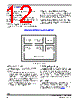
12 / 25 page  Analog Integrated Circuit Device Data 12 Freescale Semiconductor 34717 FUNCTIONAL DESCRIPTION FUNCTIONAL INTERNAL BLOCK DESCRIPTION delay and must be pulled up by an external resistor to a supply voltage like VIN. SHUTDOWN INPUT (SD) If this pin is tied to the GND pin, the device will be in Shutdown Mode. If left unconnected or tied to the VIN pin, the device will be in Normal Mode. The pin has an internal pull up of 1.5 M Ω. REFERENCE VOLTAGE INPUT (VREFIN) The output of channel two will track the voltage applied at this pin. FREQUENCY ADJUSTMENT INPUT (FREQ) The buck converters switching frequency can be adjusted by connecting this pin to an external resistor divider between VDDI and GND pins. The default switching frequency (FREQ pin connected to ground, GND) is set at 1.0 MHz. SOFT START ADJUSTMENT INPUT (ILIM1, ILIM2) Soft Start can be adjusted by applying a voltage between 1.25V and VDDI on each ILIM pin. FUNCTIONAL INTERNAL BLOCK DESCRIPTION Figure 4. Block Illustration INTERNAL BIAS CIRCUITS This block contains all circuits that provide the necessary supply voltages and bias currents for the internal circuitry. It consists of: • Internal Voltage Supply Regulator: This regulator supplies the VDDI voltage that is used to drive the digital/ analog internal circuits. It is equipped with a Power-On- Reset (POR) circuit that watches for the right regulation levels. External filtering is needed on the VDDI pin. This block will turn off during the shutdown mode. • Internal Bandgap Reference Voltage: This supplies the reference voltage to some of the internal circuitry. • Bias Circuit: This block generates the bias currents necessary to run all of the blocks in the IC. SYSTEM CONTROL AND LOGIC This block is the brain of the IC where the device processes data and reacts to it. Based on the status of the SD pin, the system control reacts accordingly and orders the device into the right status. It also takes inputs from all of the monitoring/protection circuits and initiates power up or power down commands. It communicates with the buck converter to manage the switching operation and protects it against any faults. OSCILLATOR This block generates the clock cycles necessary to run the IC digital blocks. It also generates the buck converters switching frequency. The switching frequency can be programmed by connecting a resistor divider to the FREQ pin, between VDDI and GND pins (See Figure 1). Internal Bias System Control Oscillator Circuits & Logic Control & Protection Tracking & Supervisory Functions Functions Sequencing 2 x Buck Converter |
|
|
ссылки URL |
| Вашему бизинису помогли Аллдатащит? [ DONATE ] |
Что такое Аллдатащит | реклама | контакт | Конфиденциальность | Ссылка на техническое описание | обмен ссыками | поиск по производителю All Rights Reserved©Alldatasheet.com |
| Russian : Alldatasheetru.com | Korean : Alldatasheet.co.kr | Spanish : Alldatasheet.es | French : Alldatasheet.fr | Italian : Alldatasheetit.com Portuguese : Alldatasheetpt.com | Polish : Alldatasheet.pl | Vietnamese : Alldatasheet.vn Indian : Alldatasheet.in | Mexican : Alldatasheet.com.mx | British : Alldatasheet.co.uk | New Zealand : Alldatasheet.co.nz |
|
Family Site : ic2ic.com |
icmetro.com |
 Russian ▼
 English
 Chinese
 German
 Japanese
 Russian
 Korean
 Spanish
 French
 Italian
 Portuguese
 Polish
 Vietnamese
 Indian
 Mexican
 British
 New Zealand