|
поискавой системы для электроныых деталей |
|
|
поискавой системы для электроныых деталей |
|
SI53112-A00AGM датащи(PDF) 5 Page - Skyworks Solutions Inc. |
|
|
|||||||||||||||||||||||||||||
SI53112-A00AGM датащи(HTML) 5 Page - Skyworks Solutions Inc. |
|
|
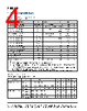
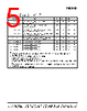
5 / 35 page  Si53112 Skyworks Solutions, Inc. • Phone [781] 376-3000 • Fax [781] 376-3100 • sales@skyworksinc.com • www.skyworksinc.com 5 Rev. 1.1 • Skyworks Proprietary Information • Products and Product Information are Subject to Change Without Notice • September 2, 2021 Table 3. Output Skew, PLL Bandwidth and Peaking TA = –40 to 85 °C; supply voltage VDD =3.3 V ±5% Parameter Test Condition Min TYP Max Unit CLK_IN, DIF[x:0] Input-to-Output Delay in PLL Mode Nominal Value1,2,3,4 –100 27 100 ps CLK_IN, DIF[x:0] Input-to-Output Delay in Bypass Mode \Nominal Value2,4,5 2.5 3.3 4.5 ns CLK_IN, DIF[x:0] Input-to-Output Delay Variation in PLL mode Over voltage and temperature2,4,5 –100 39 100 ps CLK_IN, DIF[x:0] Input-to-Output Delay Variation in Bypass Mode Over voltage and temperature2,4,5 –250 3.7 250 ps DIF[11:0] Output-to-Output Skew across all 12 Outputs (Common to Bypass and PLL Mode)1,2,3,4,5 0 20 50 ps PLL Jitter Peaking (HBW_BYPASS_LBW =0)6 — 0.4 2.0 dB PLL Jitter Peaking (HBW_BYPASS_LBW =1)6 —0.1 2.5 dB PLL Bandwidth (HBW_BYPASS_LBW =0)7 — 0.7 1.4 MHz PLL Bandwidth (HBW_BYPASS_LBW =1)7 — 2 4 MHz Notes: 1. Measured into fixed 2 pF load cap. Input-to-output skew is measured at the first output edge following the corresponding input. 2. Measured from differential cross-point to differential cross-point. 3. This parameter is deterministic for a given device. 4. Measured with scope averaging on to find mean value. 5. All Bypass Mode Input-to-Output specs refer to the timing between an input edge and the specific output edge created by it. 6. Measured as maximum pass band gain. At frequencies within the loop BW, highest point of magnification is called PLL jitter peaking. 7. Measured at 3 db down or half power point. |
|
ссылки URL |
| Вашему бизинису помогли Аллдатащит? [ DONATE ] |
Что такое Аллдатащит | реклама | контакт | Конфиденциальность | Ссылка на техническое описание | обмен ссыками | поиск по производителю All Rights Reserved©Alldatasheet.com |
| Russian : Alldatasheetru.com | Korean : Alldatasheet.co.kr | Spanish : Alldatasheet.es | French : Alldatasheet.fr | Italian : Alldatasheetit.com Portuguese : Alldatasheetpt.com | Polish : Alldatasheet.pl | Vietnamese : Alldatasheet.vn Indian : Alldatasheet.in | Mexican : Alldatasheet.com.mx | British : Alldatasheet.co.uk | New Zealand : Alldatasheet.co.nz |
|
Family Site : ic2ic.com |
icmetro.com |
 Russian ▼
 English
 Chinese
 German
 Japanese
 Russian
 Korean
 Spanish
 French
 Italian
 Portuguese
 Polish
 Vietnamese
 Indian
 Mexican
 British
 New Zealand