|
поискавой системы для электроныых деталей |
|
|
поискавой системы для электроныых деталей |
|
SI53112-A00AGM датащи(PDF) 33 Page - Skyworks Solutions Inc. |
|
|
|||||||||||||||||||||||||||||
SI53112-A00AGM датащи(HTML) 33 Page - Skyworks Solutions Inc. |
|
|
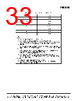
33 / 35 page  Si53112 Skyworks Solutions, Inc. • Phone [781] 376-3000 • Fax [781] 376-3100 • sales@skyworksinc.com • www.skyworksinc.com 33 Rev. 1.1 • Skyworks Proprietary Information • Products and Product Information are Subject to Change Without Notice • September 2, 2021 Table 27. PCB Land Pattern Dimensions Dimension mm C1 8.90 C2 8.90 E0.50 X1 0.30 Y1 0.85 X2 6.20 Y2 6.20 Notes: General 1. All dimensions shown are in millimeters (mm). 2. This Land Pattern Design is based on the IPC-7351 guidelines. 3. All dimensions shown are at Maximum Material Condition (MMC). Least Material Condition (LMC) is calculated based on a Fabrication Allowance of 0.05 mm. Solder Mask Design 4. All metal pads are to be non-solder mask defined (NSMD). Clearance between the solder mask and the metal pad is to be 60 m minimum, all the way around the pad. Stencil Design 5. A stainless steel, laser-cut and electro-polished stencil with trapezoidal walls should be used to assure good solder paste release. 6. The stencil thickness should be 0.125 mm (5 mils). 7. The ratio of stencil aperture to land pad size should be 1:1 for all pads. 8. A 3x3 array of 1.45 mm square openings on a 2.00 mm pitch should be used for the center ground pad. Card Assembly 9. A No-Clean, Type-3 solder paste is recommended. 10. The recommended card reflow profile is per the JEDEC/IPC J-STD-020 specification for Small Body Components. |
|
ссылки URL |
| Вашему бизинису помогли Аллдатащит? [ DONATE ] |
Что такое Аллдатащит | реклама | контакт | Конфиденциальность | Ссылка на техническое описание | обмен ссыками | поиск по производителю All Rights Reserved©Alldatasheet.com |
| Russian : Alldatasheetru.com | Korean : Alldatasheet.co.kr | Spanish : Alldatasheet.es | French : Alldatasheet.fr | Italian : Alldatasheetit.com Portuguese : Alldatasheetpt.com | Polish : Alldatasheet.pl | Vietnamese : Alldatasheet.vn Indian : Alldatasheet.in | Mexican : Alldatasheet.com.mx | British : Alldatasheet.co.uk | New Zealand : Alldatasheet.co.nz |
|
Family Site : ic2ic.com |
icmetro.com |
 Russian ▼
 English
 Chinese
 German
 Japanese
 Russian
 Korean
 Spanish
 French
 Italian
 Portuguese
 Polish
 Vietnamese
 Indian
 Mexican
 British
 New Zealand