|
поискавой системы для электроныых деталей |
|
|
поискавой системы для электроныых деталей |
|
ADL5565ACPZ-R7 датащи(PDF) 18 Page - Analog Devices |
|
|
|||||||||||||||||||||||||||||
ADL5565ACPZ-R7 датащи(HTML) 18 Page - Analog Devices |
|
|
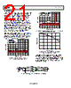
18 / 29 page  Data Sheet ADL5565 APPLICATIONS INFORMATION BASIC CONNECTIONS Figure 31 shows the basic connections for operating the ADL5565. Apply a voltage between 3 V and 5 V to the VCC pins, and decouple each supply pin with at least one low inductance, 0.1 µF surface-mount ceramic capacitor, placed as close as possible to the device. Also, decouple the VCOM pin (Pin 9) using a 0.1 µF capacitor. The gain of the part is determined by the pin-strappable input configuration. When Input A is applied to VIP1 and Input B is applied to VIN1, the gain is 6 dB (minimum gain, see Equation 1 and Equation 2). When Input A is applied to VIP2 and Input B is applied to VIN2, the gain is 12 dB (middle gain). When Input A is applied to both VIP1 and VIP2 and Input B is applied to both VIN1 and VIN2, the gain is 15.5 dB (maximum gain). Pin 1 to Pin 4, Pin 10, and Pin 11 are biased at 1/2 VCC above ground and can be dc-coupled (if within the specified input or output common-mode voltage levels) or ac-coupled as shown in Figure 31. To enable the ADL5565, the ENBL pin must be pulled high. Pulling the ENBL pin low puts the ADL5565 in sleep mode, reducing the current consumption to 5 mA at ambient. 1 2 3 4 11 12 10 9 5 6 7 8 15 16 14 13 VIP2 VIP1 VIN1 VIN2 VOP ENBL VON VCOM VCC VCC VCC VCC AC VCC GND GND GND GND ADL5565 VCC BALANCED LOAD RL 0.1µF 0.1µF 0.1µF A B 0.1µF 0.1µF 0.1µF 10µF 0.1µF RS/2 RS/2 BALANCED SOURCE Figure 31. Basic Connections Rev. E | Page 17 of 28 |
|
ссылки URL |
| Вашему бизинису помогли Аллдатащит? [ DONATE ] |
Что такое Аллдатащит | реклама | контакт | Конфиденциальность | Ссылка на техническое описание | обмен ссыками | поиск по производителю All Rights Reserved©Alldatasheet.com |
| Russian : Alldatasheetru.com | Korean : Alldatasheet.co.kr | Spanish : Alldatasheet.es | French : Alldatasheet.fr | Italian : Alldatasheetit.com Portuguese : Alldatasheetpt.com | Polish : Alldatasheet.pl | Vietnamese : Alldatasheet.vn Indian : Alldatasheet.in | Mexican : Alldatasheet.com.mx | British : Alldatasheet.co.uk | New Zealand : Alldatasheet.co.nz |
|
Family Site : ic2ic.com |
icmetro.com |
 Russian ▼
 English
 Chinese
 German
 Japanese
 Russian
 Korean
 Spanish
 French
 Italian
 Portuguese
 Polish
 Vietnamese
 Indian
 Mexican
 British
 New Zealand