|
поискавой системы для электроныых деталей |
|
|
поискавой системы для электроныых деталей |
|
TSH80DT датащи(PDF) 18 Page - STMicroelectronics |
|
|
|||||||||||||||||||||||||||||
TSH80DT датащи(HTML) 18 Page - STMicroelectronics |
|
|
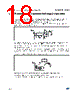
18 / 23 page  Precautions on Asymmetrical Supply Operation TSH80-TSH81-TSH82 18/23 5 Precautions on Asymmetrical Supply Operation The TSH8X can be used either with a dual or a single supply. If a single supply is used, the inputs are biased to the mid-supply voltage (+Vcc/2). This bias network must be carefully designed, in order to reject any noise present on the supply rail. As the bias current is 15uA, you must carefully choose the resistance R1 not to introduce an offset mismatch at the amplifier inputs. R1=10k Ω will be convenient. C1, C2, C3 are bypass capacitors from perturbation on Vcc as well as for the input and output signals. We choose C1=100nF and C2=C3=100uF. R2, R3 are such that the current through them must be superior to 100 times the bias current. So, we take R2=R3=4.7k Ω. Cin, as Cout are chosen to filter the DC signal by the low pass filters (R1,Cin) and (Rout, Cout). By taking R1=10k Ω, RL=150Ω, and Cin=2uF, Cout=220uF we provide a cutoff frequency below 10Hz. Some precautions have to be added, specially for low power supply application. A feedback capacitance Cf should be added for better stability. The table summarizes the impact of the capacitance Cf on the phase margin of the circuit. Figure 33. Use of the TSH8x in gain = -1 configuration IN R1 Vcc+ OUT R2 R3 C1 C3 C2 Cin Cout + - Cf R5 R4 RL IN R1 Vcc+ OUT R2 R3 C1 C3 C2 Cin Cout + - 1k Cf 1k RL |
|
|
ссылки URL |
| Вашему бизинису помогли Аллдатащит? [ DONATE ] |
Что такое Аллдатащит | реклама | контакт | Конфиденциальность | Ссылка на техническое описание | обмен ссыками | поиск по производителю All Rights Reserved©Alldatasheet.com |
| Russian : Alldatasheetru.com | Korean : Alldatasheet.co.kr | Spanish : Alldatasheet.es | French : Alldatasheet.fr | Italian : Alldatasheetit.com Portuguese : Alldatasheetpt.com | Polish : Alldatasheet.pl | Vietnamese : Alldatasheet.vn Indian : Alldatasheet.in | Mexican : Alldatasheet.com.mx | British : Alldatasheet.co.uk | New Zealand : Alldatasheet.co.nz |
|
Family Site : ic2ic.com |
icmetro.com |
 Russian ▼
 English
 Chinese
 German
 Japanese
 Russian
 Korean
 Spanish
 French
 Italian
 Portuguese
 Polish
 Vietnamese
 Indian
 Mexican
 British
 New Zealand