|
поискавой системы для электроныых деталей |
|
|
поискавой системы для электроныых деталей |
|
CM339CS датащи(PDF) 4 Page - List of Unclassifed Manufacturers |
|
|
|||||||||||||||||||||||||||||
CM339CS датащи(HTML) 4 Page - List of Unclassifed Manufacturers |
|
|
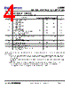
4 / 7 page  CM339 LOW POWER QUAD VOLTAGE COMPARATORS 2001/07/02 Preliminary Champion Microelectronic Corporation Page 3 ELECTRICAL CHARACTERISTICS Vcc + = +5V, Vcc+ = GND, T amb=25℃(Unless otherwise specified) CM339 Symbol Parameter Min. Typ. Max. Units Vio Input offset voltage-(note 1) Tamb = +25℃ Tmin ≤ Tamb ≤ Tmax 1.0 2.2 MV Iio Input offset current Tamb = +25℃ Tmin ≤ Tamb ≤ Tmax 5.0 50 nA Iio Input bias current Tamb = +25℃ Tmin ≤ Tamb ≤ Tmax 25 250 nA Avd Large signal voltage gain (Vcc = 15, RL = 15k Ω, Vo = 1 to 11V) 50 200 V/mV Icc Supply current(all comparators) Vcc = +5V, no load Vcc = +30V, no load 0.8 2.0 mA Vicm Input common mode voltage range-(note 2) (Vcc = 30V) Tamb = +25℃ Tmin ≤ Tamb ≤ Tmax 0 Vcc + - 1.5 V Vid Differential input voltage -(note 4) 36 V Isink Output sink current (Vid = -1V, Vo = 1.5V) 6.0 16 mA tre Response Time -(note 3) (RL = 5.1k Ω connected to Vcc+) 1.3 μs trel Large signal response time (RL = 5.1k Ω connected to Vcc+, ei = TTL, V(ref))= +1.4V) 300 ns Notes : 1.At output switch point, Vo = 1.4V, Rs = 0 with Vcc + from 5V to 30V, and over the full input common-mode range(0V to Vcc + -1.5V). 2.The input common-mode voltage of the either input signal voltage should not be allowed to go negative by more than 0.3V. The upper and of the common-mode voltage range is Vcc + -1.5V, but either or both inputs can go to +30V without damage. 3.The response time specified is for a 100mV input step with 5mV overdrive. For larger overdrive signals 300ns can be obtained. 4.Positive excursions of input voltage may power supply level. As long as the other voltage remains within the common-mode range, the comparator will provide a proper output state. The low input voltage state must not be less than –0.3V(or 0.3V bellow the negative power supply, if used). |
|
|
ссылки URL |
| Вашему бизинису помогли Аллдатащит? [ DONATE ] |
Что такое Аллдатащит | реклама | контакт | Конфиденциальность | Ссылка на техническое описание | обмен ссыками | поиск по производителю All Rights Reserved©Alldatasheet.com |
| Russian : Alldatasheetru.com | Korean : Alldatasheet.co.kr | Spanish : Alldatasheet.es | French : Alldatasheet.fr | Italian : Alldatasheetit.com Portuguese : Alldatasheetpt.com | Polish : Alldatasheet.pl | Vietnamese : Alldatasheet.vn Indian : Alldatasheet.in | Mexican : Alldatasheet.com.mx | British : Alldatasheet.co.uk | New Zealand : Alldatasheet.co.nz |
|
Family Site : ic2ic.com |
icmetro.com |
 Russian ▼
 English
 Chinese
 German
 Japanese
 Russian
 Korean
 Spanish
 French
 Italian
 Portuguese
 Polish
 Vietnamese
 Indian
 Mexican
 British
 New Zealand