|
поискавой системы для электроныых деталей |
|
|
поискавой системы для электроныых деталей |
|
AD627ARZ-R7 датащи(PDF) 17 Page - Analog Devices |
|
|
|||||||||||||||||||||||||||||
AD627ARZ-R7 датащи(HTML) 17 Page - Analog Devices |
|
|
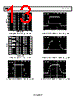
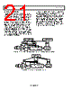
17 / 25 page  AD627 Data Sheet Rev. E | Page 16 of 24 Table 6. Recommended Values of Gain Resistors Desired Gain 1% Standard Table Value of RG Resulting Gain 5 ∞ 5.00 6 200 kΩ 6.00 7 100 kΩ 7.00 8 68.1 kΩ 7.94 9 51.1 kΩ 8.91 10 40.2 kΩ 9.98 15 20 kΩ 15.00 20 13.7 kΩ 19.60 25 10 kΩ 25.00 30 8.06 kΩ 29.81 40 5.76 kΩ 39.72 50 4.53 kΩ 49.15 60 3.65 kΩ 59.79 70 3.09 kΩ 69.72 80 2.67 kΩ 79.91 90 2.37 kΩ 89.39 100 2.1 kΩ 100.24 200 1.05 kΩ 195.48 500 412 Ω 490.44 1000 205 Ω 980.61 REFERENCE TERMINAL The reference terminal potential defines the zero output voltage and is especially useful when the load does not share a precise ground with the rest of the system. It provides a direct means of injecting a precise offset to the output. The reference terminal is also useful when amplifying bipolar signals, because it provides a virtual ground voltage. The AD627 output voltage is developed with respect to the poten- tial on the reference terminal; therefore, tying the REF pin to the appropriate local ground solves many grounding problems. For optimal CMR, tie the REF pin to a low impedance point. INPUT RANGE LIMITATIONS IN SINGLE-SUPPLY APPLICATIONS In general, the maximum achievable gain is determined by the available output signal range. However, in single-supply applica- tions where the input common-mode voltage is nearly or equal to 0, some limitations on the gain can be set. Although the Specifications section nominally defines the input, output, and reference pin ranges, the voltage ranges on these pins are mutually interdependent. Figure 37 shows the simplified schematic of the AD627, driven by a differential voltage (VDIFF) that has a common-mode component, VCM. The voltage on the A1 op amp output is a function of VDIFF, VCM, the voltage on the REF pin, and the programmed gain. This voltage is given by VA1 = 1.25 (VCM + 0.5 V) − 0.25 VREF − VDIFF (25 kΩ/RG + 0.625) (3) The voltage on A1 can also be expressed as a function of the actual voltages on the –IN and +IN pins (V− and V+) such that VA1 = 1.25 ((V−) + 0.5 V) − 0.25 VREF − ((V+) − (V−)) 25 kΩ/RG (4) The output of A1 is capable of swinging to within 50 mV of the negative rail and to within 200 mV of the positive rail. It is clear, from either Equation 3 or Equation 4, that an increasing VREF (while it acts as a positive offset at the output of the AD627) tends to decrease the voltage on A1. Figure 38 and Figure 39 show the maximum voltages that can be applied to the REF pin for a gain of 5 for both the single-supply and dual-supply cases. VIN(–) (V) 5 –6 4 3 2 1 0 –1 –2 –3 –4 –5 –5 –4 –3 –2 –1 0 1 2 3 4 MAXIMUM VREF MINIMUM VREF Figure 38. Reference Input Voltage vs. Negative Input Voltage, VS = ±5 V, G = +5 VIN(–) (V) 5 –0.5 4 3 2 1 0 0 0.5 1.0 2.0 1.5 2.5 3.0 3.5 4.0 4.5 MAXIMUM VREF MINIMUM VREF Figure 39. Reference Input Voltage vs. Negative Input Voltage, VS = 5 V, G = +5 Raising the input common-mode voltage increases the voltage on the output of A1. However, in single-supply applications where the common-mode voltage is low, a differential input voltage or a voltage on REF that is too high can drive the output of A1 into the ground rail. Some low-side headroom is added because both inputs are shifted upwards by about 0.5 V (that is, by the VBE of Q1 and Q2). Use Equation 3 and Equation 4 to check whether the voltage on Amplifier A1 is within its operating range. |
|
|
ссылки URL |
| Вашему бизинису помогли Аллдатащит? [ DONATE ] |
Что такое Аллдатащит | реклама | контакт | Конфиденциальность | Ссылка на техническое описание | обмен ссыками | поиск по производителю All Rights Reserved©Alldatasheet.com |
| Russian : Alldatasheetru.com | Korean : Alldatasheet.co.kr | Spanish : Alldatasheet.es | French : Alldatasheet.fr | Italian : Alldatasheetit.com Portuguese : Alldatasheetpt.com | Polish : Alldatasheet.pl | Vietnamese : Alldatasheet.vn Indian : Alldatasheet.in | Mexican : Alldatasheet.com.mx | British : Alldatasheet.co.uk | New Zealand : Alldatasheet.co.nz |
|
Family Site : ic2ic.com |
icmetro.com |
 Russian ▼
 English
 Chinese
 German
 Japanese
 Russian
 Korean
 Spanish
 French
 Italian
 Portuguese
 Polish
 Vietnamese
 Indian
 Mexican
 British
 New Zealand