|
поискавой системы для электроныых деталей |
|
|
поискавой системы для электроныых деталей |
|
82C55A датащи(PDF) 3 Page - Harris Corporation |
|
|
|||||||||||||||||||||||||||||
82C55A датащи(HTML) 3 Page - Harris Corporation |
|
|
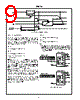
3 / 26 page  3 Functional Description Data Bus Buffer This three-state bi-directional 8-bit buffer is used to interface the 82C55A to the system data bus. Data is transmitted or received by the buffer upon execution of input or output instructions by the CPU. Control words and status informa- tion are also transferred through the data bus buffer. Read/Write and Control Logic The function of this block is to manage all of the internal and external transfers of both Data and Control or Status words. It accepts inputs from the CPU Address and Control busses and in turn, issues commands to both of the Control Groups. (CS) Chip Select. A “low” on this input pin enables the communcation between the 82C55A and the CPU. (RD) Read. A “low” on this input pin enables 82C55A to send the data or status information to the CPU on the data bus. In essence, it allows the CPU to “read from” the 82C55A. (WR) Write. A “low” on this input pin enables the CPU to write data or control words into the 82C55A. (A0 and A1) Port Select 0 and Port Select 1. These input signals, in conjunction with the RD and WR inputs, control the selection of one of the three ports or the control word register. They are normally connected to the least significant bits of the address bus (A0 and A1). (RESET) Reset. A “high” on this input initializes the control register to 9Bh and all ports (A, B, C) are set to the input mode. “Bus hold” devices internal to the 82C55A will hold the I/O port inputs to a logic “1” state with a maximum hold current of 400 µA. Group A and Group B Controls The functional configuration of each port is programmed by the systems software. In essence, the CPU “outputs” a con- trol word to the 82C55A. The control word contains information such as “mode”, “bit set”, “bit reset”, etc., that ini- tializes the functional configuration of the 82C55A. Each of the Control blocks (Group A and Group B) accepts “commands” from the Read/Write Control logic, receives “control words” from the internal data bus and issues the proper commands to its associated ports. Control Group A - Port A and Port C upper (C7 - C4) Control Group B - Port B and Port C lower (C3 - C0) The control word register can be both written and read as shown in the “Basic Operation” table. Figure 4 shows the control word format for both Read and Write operations. When the control word is read, bit D7 will always be a logic “1”, as this implies control word mode information. 82C55A BASIC OPERATION A1 A0 RD WR CS INPUT OPERATION (READ) 00010 Port A → Data Bus 01010 Port B → Data Bus 10010 Port C → Data Bus 11010 Control Word → Data Bus OUTPUT OPERATION (WRITE) 00100 Data Bus → Port A 01100 Data Bus → Port B 10100 Data Bus → Port C 11100 Data Bus → Control DISABLE FUNCTION XXXX 1 Data Bus → Three-State X X 1 1 0 Data Bus → Three-State FIGURE 1. 82C55A BLOCK DIAGRAM. DATA BUS BUFFER, READ/WRITE, GROUP A & B CONTROL LOGIC FUNCTIONS GROUP A PORT A (8) GROUP A PORT C UPPER (4) GROUP B PORT C LOWER (4) GROUP B PORT B (8) GROUP B CONTROL GROUP A CONTROL DATA READ WRITE CONTROL LOGIC RD WR A1 A0 RESET CS D7-D0 POWER SUPPLIES +5V GND BI-DIRECTIONAL DATA BUS I/O PA7- I/O PC7- I/O PC3- I/O PB7- BUFFER BUS PB0 PC0 PC4 PA0 8-BIT INTERNAL DATA BUS 82C55A |
|
|
ссылки URL |
| Вашему бизинису помогли Аллдатащит? [ DONATE ] |
Что такое Аллдатащит | реклама | контакт | Конфиденциальность | Ссылка на техническое описание | обмен ссыками | поиск по производителю All Rights Reserved©Alldatasheet.com |
| Russian : Alldatasheetru.com | Korean : Alldatasheet.co.kr | Spanish : Alldatasheet.es | French : Alldatasheet.fr | Italian : Alldatasheetit.com Portuguese : Alldatasheetpt.com | Polish : Alldatasheet.pl | Vietnamese : Alldatasheet.vn Indian : Alldatasheet.in | Mexican : Alldatasheet.com.mx | British : Alldatasheet.co.uk | New Zealand : Alldatasheet.co.nz |
|
Family Site : ic2ic.com |
icmetro.com |
 Russian ▼
 English
 Chinese
 German
 Japanese
 Russian
 Korean
 Spanish
 French
 Italian
 Portuguese
 Polish
 Vietnamese
 Indian
 Mexican
 British
 New Zealand