|
поискавой системы для электроныых деталей |
|
|
поискавой системы для электроныых деталей |
|
TC820 датащи(PDF) 21 Page - Microchip Technology |
|
|
|||||||||||||||||||||||||||||
TC820 датащи(HTML) 21 Page - Microchip Technology |
|
|
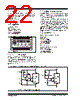
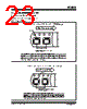
21 / 28 page  © 2002 Microchip Technology Inc. DS21476B-page 21 TC820 5.11 External Peak Detection The TC820 will hold the highest A/D conversion or fre- quency reading indefinitely when the PKHOLD input is connected to VDD. However, the analog peak input must be present during the A/D converter's signal inte- grate period. For slowly changing signals, such as tem- perature, the peak reading will be properly converted and held. If rapidly changing analog signals must be held, an external peak detector should be added. An inexpensive circuit can be made from an op amp and a few discrete components, as shown in Figure 5-12. The droop rate of the external peak detector should be adjusted so that the held voltage will not decay below the desired accuracy level during the converter's 400msec conversion time. FIGURE 5-12: EXTERNAL PEAK DETECTOR 5.12 Liquid Crystal Display (LCD) The TC820 drives a triplex (multiplexed 3:1) LCD with three backplanes. The LCD can include decimal points, polarity sign, and annunciators for over range, peak hold, high and low logic levels, and low battery. Table 5-2 shows the assignment of the display seg- ments to the backplanes and segment drive lines. The backplane drive frequency is obtained by dividing the oscillator frequency by 240. Backplane waveforms are shown in Figure 5-13. These appear on outputs BP1, BP2, and BP3. They remain the same, regardless of the segments being driven. FIGURE 5-13: BACKPLANE WAVEFORMS Other display output lines have waveforms that vary depending on the displays values. Figure 5-13 shows a set of waveforms for the a, g, d outputs of one digit for several combinations of "on" segments. FIGURE 5-14: TYPICAL DISPLAY OUTPUT WAVEFORMS TABLE 5-2: LCD BACKPLANE AND SEGMENT ASSIGNMENTS *Connect both pins 2 and 16 of LCD to TC820 BP3 of output. VDD TC820 VSS VIN+ PKHOLD 0V 0.01µF Offset Null 1N4148 +9V 10k Ω VIN TL061 BP1 BP2 BP3 40-Pin (PDIP) 44-Pin (PQFP) LCD Display Pin Number BP1 BP2 BP3 140 3 LOW 241 4 A4 "—" 3 42 5 B4 G4 E4 4 43 6 HIGH C4 D4 544 7 A3 F3 DP3 61 8 B3 G3 E3 7 2 9 OVER C3 D3 83 10 A2 F2 DP2 9 4 11 B2 G2 E2 10 5 12 PEAK C2 D2 11 6 13 A1 F1 DP1 12 7 14 B1 G1 E1 13 8 2,16* — C1 D1 14 9 1 BP1 — BATT 15 10 15 LOW BP2 BP3 VDD VH VL VDISP VDD VH VL VDISP VDD VH VL VDISP VDD VH VL VDISP Segment Line All OFF a Segment ON d, g OFF a, g ON d OFF All ON |
|
ссылки URL |
| Вашему бизинису помогли Аллдатащит? [ DONATE ] |
Что такое Аллдатащит | реклама | контакт | Конфиденциальность | Ссылка на техническое описание | обмен ссыками | поиск по производителю All Rights Reserved©Alldatasheet.com |
| Russian : Alldatasheetru.com | Korean : Alldatasheet.co.kr | Spanish : Alldatasheet.es | French : Alldatasheet.fr | Italian : Alldatasheetit.com Portuguese : Alldatasheetpt.com | Polish : Alldatasheet.pl | Vietnamese : Alldatasheet.vn Indian : Alldatasheet.in | Mexican : Alldatasheet.com.mx | British : Alldatasheet.co.uk | New Zealand : Alldatasheet.co.nz |
|
Family Site : ic2ic.com |
icmetro.com |
 Russian ▼
 English
 Chinese
 German
 Japanese
 Russian
 Korean
 Spanish
 French
 Italian
 Portuguese
 Polish
 Vietnamese
 Indian
 Mexican
 British
 New Zealand