|
поискавой системы для электроныых деталей |
|
|
поискавой системы для электроныых деталей |
|
MAX5250 датащи(PDF) 10 Page - Maxim Integrated Products |
|
|
|||||||||||||||||||||||||||||
MAX5250 датащи(HTML) 10 Page - Maxim Integrated Products |
|
|
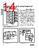
10 / 16 page  Figure 5 shows the serial-interface timing requirements. The chip-select pin ( CS) must be low to enable the DAC’s serial interface. When CS is high, the interface control circuitry is disabled. CS must go low at least tCSS before the rising serial clock (SCLK) edge to prop- erly clock in the first bit. When CS is low, data is clocked into the internal shift register via the serial-data input pin (DIN) on SCLK’s rising edge. The maximum guaranteed clock frequency is 10MHz. Data is latched into the appropriate MAX5250 input/DAC registers on CS’s rising edge. The programming command Load-All-DACs-From-Shift- Register allows all input and DAC registers to be simul- taneously loaded with the same digital code from the input shift register. The no operation (NOP) command leaves the register contents unaffected and is useful when the MAX5250 is configured in a daisy chain (see the Daisy Chaining Devices section). The command to change the clock edge on which serial data is shifted out of DOUT also loads data from all input registers to their respective DAC registers. Serial-Data Output (DOUT) The serial-data output, DOUT, is the internal shift regis- ter’s output. The MAX5250 can be programmed so that data is clocked out of DOUT on SCLK’s rising edge (Mode 1) or falling edge (Mode 0). In Mode 0, output data at DOUT lags input data at DIN by 16.5 clock cycles, maintaining compatibility with Microwire, SPI/QSPI, and other serial interfaces. In Mode 1, output data lags input data by 16 clock cycles. On power-up, DOUT defaults to Mode 0 timing. User-Programmable Logic Output (UPO) The user-programmable logic output, UPO, allows an external device to be controlled via the MAX5250 serial interface (Table 1). Low-Power, Quad, 10-Bit Voltage-Output DAC with Serial Interface 10 ______________________________________________________________________________________ Table 1. Serial-Interface Programming Commands “X” = Don’t care 16-BIT SERIAL WORD FUNCTION A1 A0 C1 C0 D9.................D0 MSB.............LSB S1 S0 00 01 10 11 01 01 01 01 10-bit DAC data 10-bit DAC data 10-bit DAC data 10-bit DAC data 00 00 00 00 Load input register A; DAC registers unchanged. Load input register B; DAC registers unchanged. Load input register C; DAC registers unchanged. Load input register D; DAC registers unchanged. 00 01 10 11 11 11 11 11 10-bit DAC data 10-bit DAC data 10-bit DAC data 10-bit DAC data 00 00 00 00 Load input register A; all DAC registers updated. Load input register B; all DAC registers updated. Load input register C; all DAC registers updated. Load input register D; all DAC registers updated. 01 00 XXXXXXXXXX XX Update all DAC registers from their respective input registers (also exit shutdown mode). 10 00 10-bit DAC data 00 Load all DAC registers from shift register (also exit shutdown mode). 11 00 XXXXXXXXXX XX Enter shutdown mode (provided PDL = 1). 00 10 XXXXXXXXXX XX UPO goes low (default). 01 10 XXXXXXXXXX XX UPO goes high. 00 00 XXXXXXXXXX XX No operation (NOP) to DAC registers 11 10 XXXXXXXXXX XX Mode 1, DOUT clocked out on SCLK’s rising edge. All DAC registers updated. 10 10 XXXXXXXXXX XX Mode 0, DOUT clocked out on SCLK’s falling edge. All DAC registers updated (default). |
|
|
ссылки URL |
| Вашему бизинису помогли Аллдатащит? [ DONATE ] |
Что такое Аллдатащит | реклама | контакт | Конфиденциальность | Ссылка на техническое описание | обмен ссыками | поиск по производителю All Rights Reserved©Alldatasheet.com |
| Russian : Alldatasheetru.com | Korean : Alldatasheet.co.kr | Spanish : Alldatasheet.es | French : Alldatasheet.fr | Italian : Alldatasheetit.com Portuguese : Alldatasheetpt.com | Polish : Alldatasheet.pl | Vietnamese : Alldatasheet.vn Indian : Alldatasheet.in | Mexican : Alldatasheet.com.mx | British : Alldatasheet.co.uk | New Zealand : Alldatasheet.co.nz |
|
Family Site : ic2ic.com |
icmetro.com |
 Russian ▼
 English
 Chinese
 German
 Japanese
 Russian
 Korean
 Spanish
 French
 Italian
 Portuguese
 Polish
 Vietnamese
 Indian
 Mexican
 British
 New Zealand