|
поискавой системы для электроныых деталей |
|
|
поискавой системы для электроныых деталей |
|
IR3553 датащи(PDF) 4 Page - International Rectifier |
|
|
|||||||||||||||||||||||||||||
IR3553 датащи(HTML) 4 Page - International Rectifier |
|
|
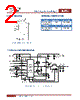
4 / 22 page  July 16, 2014 | DATASHEET V3.3 4 IR3553 40A Integrated PowIRstage® PIN DESCRIPTIONS PIN # PIN NAME PIN DESCRIPTION 1 CSIN- Inverting input to the current sense amplifier. Connect to LGND if the current sense amplifier is not used. 2 CSIN+ Non-Inverting input to the current sense amplifier. Connect to LGND if the current sense amplifier is not used. 3 VCC Bias voltage for control logic. Connect a minimum 1uF cap between VCC and PGND (pin 4) if current sense amplifier is used. Connect a minimum 0.22uF capacitor between VCC and PGND (pin 4) if current sense amplifier is not used. 4, 12, 13 PGND Power ground of MOSFET driver and the synchronous MOSFET. MOSFET driver signal is referenced to this pin. 5, 25 GATEL Low-side MOSFET driver pins that can be connected to a test point in order to observe the waveform. 6 – 11 SW Switch node of synchronous buck converter. 14 – 16 VIN High current input voltage connection. Recommended operating range is 4.5V to 15V. Connect at least two 10uF 1206 ceramic capacitors and a 0.22uF 0402 ceramic capacitor. Place the capacitors as close as possible to VIN pins and PGND pins (12-13). The 0.22uF 0402 capacitor should be on the same side of the PCB as the IR3553. 17 BOOST Bootstrap capacitor connection. The bootstrap capacitor provides the charge to turn on the control MOSFET. Connect a minimum 0.22µF capacitor from BOOST to SW pin. Place the capacitor as close to BOOST pin as possible and minimize parasitic inductance of PCB routing from the capacitor to SW pin. 18 PHSFLT# Open drain output of the phase fault circuits. Connect to an external pull-up resistor. Output is low when a MOSFET fault or over temperature condition is detected. 19 PWM 3.3V logic level tri-state PWM input and 7V tolerant. “High” turns the control MOSFET on, and “Low” turns the synchronous MOSFET on. “Tri-state” turns both MOSFETs off in Body-Braking® mode. In diode emulation mode, “Tri-state” activates internal diode emulation control. See “PWM Tri-state Input” Section for further details about the PWM Tri-State functions. 20 BBRK# 3.3V logic level input and 7V tolerant with internal weak pull-up to 3.3V. Logic low disables both MOSFETs. Pull up to VCC directly or by a 4.7kΩ resistor if Body-Braking® is not used. The second function of the BBRK# pin is to select diode emulatiom mode. Pulling BBRK# low at least 20ns after VCC passes its UVLO threshold selects internal diode emulation control. See “Body-Braking ® Mode” Section for further details. 21 LGND Signal ground. Driver control logic, analog circuits and IC substrate are referenced to this pin. 22 REFIN Reference voltage input from the PWM controller. IOUT signal is referenced to the voltage on this pin. Connect to LGND if the current sense amplifier is not used. 23 IOUT Current output signal. Voltage on this pin is equal to V(REFIN) + 32.5 * [V(CSIN+) – V(CSIN-)]. Float this pin if the current sense amplifier is not used. 24 TGND This pin is connected to internal power and signal ground of the driver. For best performance of the current sense amplifier, TGND must be electrically isolated from Power Ground (PGND) and Signal Ground (LGND) in the PCB layout. Connect to PGND if the current sense amplifier is not used. |
|
|
ссылки URL |
| Вашему бизинису помогли Аллдатащит? [ DONATE ] |
Что такое Аллдатащит | реклама | контакт | Конфиденциальность | Ссылка на техническое описание | обмен ссыками | поиск по производителю All Rights Reserved©Alldatasheet.com |
| Russian : Alldatasheetru.com | Korean : Alldatasheet.co.kr | Spanish : Alldatasheet.es | French : Alldatasheet.fr | Italian : Alldatasheetit.com Portuguese : Alldatasheetpt.com | Polish : Alldatasheet.pl | Vietnamese : Alldatasheet.vn Indian : Alldatasheet.in | Mexican : Alldatasheet.com.mx | British : Alldatasheet.co.uk | New Zealand : Alldatasheet.co.nz |
|
Family Site : ic2ic.com |
icmetro.com |
 Russian ▼
 English
 Chinese
 German
 Japanese
 Russian
 Korean
 Spanish
 French
 Italian
 Portuguese
 Polish
 Vietnamese
 Indian
 Mexican
 British
 New Zealand