|
поискавой системы для электроныых деталей |
|
|
поискавой системы для электроныых деталей |
|
IDT74FST163214 датащи(PDF) 4 Page - Integrated Device Technology |
|
|
|||||||||||||||||||||||||||||
IDT74FST163214 датащи(HTML) 4 Page - Integrated Device Technology |
|
|
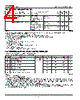
4 / 6 page  4 IDT74FST163214 12-BIT 3:1 MUX/DEMUX SWITCH COMMERCIAL TEMPERATURE RANGE POWER SUPPLY CHARACTERISTICS NOTES: 1. For conditions shown as Max. or Min., use appropriate value specified under Electrical Characteristics for the applicable device type. 2. Typical values are at VCC = 5.0V, +25 °C ambient. 3. Per TTL driven input (VIN = 3.4V). All other inputs at VCC or GND. 4. This parameter is not directly testable, but is derived for use in Total Power Supply Calculations. 5. Values for these conditions are examples of the ICC formula. These limits are guaranteed but not tested. 6. IC = IQUIESCENT + IINPUTS + IDYNAMIC IC = ICC + ∆ICC DHNT + ICCD (fiN) ICC = Quiescent Current ∆ICC = Power Supply Current for a TTL High Input (VIN = 3.4V) DH = Duty Cycle for TTL Inputs High NT = Number of TTL Inputs at DH ICCD = Dynamic Current Caused by an Input Transition Pair (HLH or LHL) fi = Input Frequency N = Number of Switches Toggling at fi All currents are in milliamps and all frequencies are in megahertz. SWITCHING CHARACTERISTICS OVER OPERATING RANGE Following Conditions Apply Unless Otherwise Specified: Commercial: TA =–40 °C to +85°C, VCC = 5.0V ±10% Symbol Parameter Test Conditions(1) Min. Typ.(2) Max. Unit ∆ICC Quiescent Power Supply Current TTL Inputs HIGH VCC = Max. VIN = 3.4V(3) — 0.5 1.5 mA ICCD Dynamic Power Supply Current(4) VCC = Max. Outputs Open VIN = VCC VIN = GND —30 40 µA/ MHz/ Enable Pin Toggling 50% Duty Cycle Switch IC Total Power Supply Current(6) VCC = Max. Outputs Open 3 Select Pins Toggling VIN = VCC VIN = GND — 3.6 4.8 mA (12 Switches Toggling) fi = 10MHz 50% Duty Cycle VIN = 3.4 VIN = GND — 4.4 7.1 3209 tbl 06 Symbol Description Condition(1) Min.(2) Typ. Max. Unit tPLH tPHL Data Propagation Delay A to B, B to A(3,4) CL = 50pF RL = 500 Ω — — 0.25 ns tBX Switch Multiplex Delay S to A, B 1.5 — 6.5 ns tPZH tPZL Switch Turn on Delay S to A, B 1.5 — 6.5 ns tPHZ tPLZ Switch Turn off Delay S to A, B 1.5 — 7 ns |QCI| Charge Injection, Typical(5,7) — 1.5 — pC |QDCI| Differential Charge Injection, Typical(6,7) — 0.5 — 3209 tbl 07 NOTES: 1. See test circuit and waveforms. 2. Minimum limits guaranteed but not tested. 3. This parameter is guaranteed by design but not tested. 4. The bus switch contributes no propagation delay other than the RC delay of the on resistance of the switch and the load capacitance. The time constant for the switch alone is of the order of 2.5ns for 50pF load. Since this time is constant and much smaller than the rise/fall times of typical driving signals, it adds very little propagation delay to the system. Propagation delay on the bus switch when used in a system is determined by the driving circuit on the driving side of the switch and its interaction with the load on the driven side. 5. Measured at switch turn off, load = 50 pF in parallel with 10 M Ω scope probe, VIN = 0.0 volts. 6. Measured at switch turn off through bus multiplexer, (e.g.- A to B1 = >A to B2), load = 50 pF in parallel with 10 M Ω scope probe, VIN at A = 0.0 volts. Charge injection is reduced because the injection from the turn off of the A to B1 switch is compensated by the turn on of the A to B2 switch. 7. Characterized parameter. Not 100% tested. |
|
|
ссылки URL |
| Вашему бизинису помогли Аллдатащит? [ DONATE ] |
Что такое Аллдатащит | реклама | контакт | Конфиденциальность | Ссылка на техническое описание | обмен ссыками | поиск по производителю All Rights Reserved©Alldatasheet.com |
| Russian : Alldatasheetru.com | Korean : Alldatasheet.co.kr | Spanish : Alldatasheet.es | French : Alldatasheet.fr | Italian : Alldatasheetit.com Portuguese : Alldatasheetpt.com | Polish : Alldatasheet.pl | Vietnamese : Alldatasheet.vn Indian : Alldatasheet.in | Mexican : Alldatasheet.com.mx | British : Alldatasheet.co.uk | New Zealand : Alldatasheet.co.nz |
|
Family Site : ic2ic.com |
icmetro.com |
 Russian ▼
 English
 Chinese
 German
 Japanese
 Russian
 Korean
 Spanish
 French
 Italian
 Portuguese
 Polish
 Vietnamese
 Indian
 Mexican
 British
 New Zealand