|
поискавой системы для электроныых деталей |
|
|
поискавой системы для электроныых деталей |
|
L8565L-S08-R датащи(PDF) 10 Page - Unisonic Technologies |
|
|
|||||||||||||||||||||||||||||
L8565L-S08-R датащи(HTML) 10 Page - Unisonic Technologies |
|
|
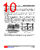
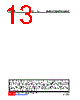
10 / 13 page  L8565 Preliminary LINEAR INTEGRATED CIRCUIT UNISONICTECHNOLOGIESCO.,LTD 10 of 13 www.unisonic.com.tw QW-R114-004.d FUNCTIONAL DESCRIPTION(Cont.) 6.2 Current Loop Compensation The compensation of the current loop is done at the ICOMP pin. This is the OTA2 output and a capacitor C3 has to be installed at this node to ground (see Fig. 10). Under normal mode of operation, this pin gives a voltage which is proportional to the averaged inductor current. This pin is internally shorted to 5V in the event of IC shuts down when OLP and UVLO occur. 6.3 Pulse Width Modulation (PWM) The IC employs an average current control scheme in continuous conduction mode (CCM) to achieve the power factor correction. Assuming the voltage loop is working and output voltage is kept constant, the off duty cycle DOFF for a CCM PFC system is given as OUT IN V V OFF = D From the above equation, DOFF is proportional to VIN. The objective of the current loop is to regulate the average inductor current such that it is proportional to the off duty cycle DOFF, and thus to the input voltage VIN. Fig. 11 shows the scheme to achieve the objective. The PWM is performed by the intersection of a ramp signal with the averaged inductor current at pin 3 (ICOMP). The PWM cycle starts with the Gate turn off for a duration of TOFF(MIN) (250ns typ.) and the ramp is kept discharged. The ramp is then allowed to rise after TOFF(MIN) expires. The off time of the boost transistor ends at the intersection of the ramp signal and the averaged current waveform. This results in the proportional relationship between the average current and the off duty cycle DOFF. Fig. 12 shows the timing diagrams of TOFF(MIN) and the PWM waveforms. ramp profile ave(IIN) at ICOMP GATE drive t Fig. 11 Average Current Control in CCM 6.4 Nonlinear Gain Block The nonlinear gain block controls the amplitude of the regulated inductor current. The input of this block is the voltage at pin VCOMP. This block has been designed to support the wide input voltage range (85-265VAC). |
|
|
ссылки URL |
| Вашему бизинису помогли Аллдатащит? [ DONATE ] |
Что такое Аллдатащит | реклама | контакт | Конфиденциальность | Ссылка на техническое описание | обмен ссыками | поиск по производителю All Rights Reserved©Alldatasheet.com |
| Russian : Alldatasheetru.com | Korean : Alldatasheet.co.kr | Spanish : Alldatasheet.es | French : Alldatasheet.fr | Italian : Alldatasheetit.com Portuguese : Alldatasheetpt.com | Polish : Alldatasheet.pl | Vietnamese : Alldatasheet.vn Indian : Alldatasheet.in | Mexican : Alldatasheet.com.mx | British : Alldatasheet.co.uk | New Zealand : Alldatasheet.co.nz |
|
Family Site : ic2ic.com |
icmetro.com |
 Russian ▼
 English
 Chinese
 German
 Japanese
 Russian
 Korean
 Spanish
 French
 Italian
 Portuguese
 Polish
 Vietnamese
 Indian
 Mexican
 British
 New Zealand